DDR DRAM IP
Filter
Compare
211
IP
from
19
vendors
(1
-
10)
-
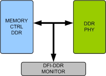
DDR DFI Verification IP
- Compliant with DFI version 2.0 or higher Specification.
- DFI-DDR Applies to :
- DDR protocol standard JESD79F Specification
- Supports all Interface Groups.
-
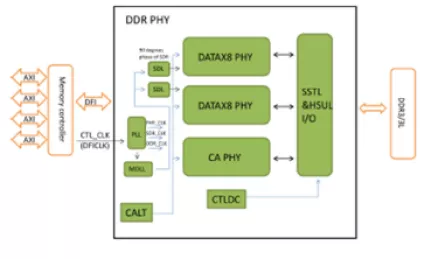
DDR and LPDDR Combo PHY
- Supports multiple combinations of DDR/LPDDR interfaces
- Compliant with JEDEC DDR and LPDDR standards
- Supports all auto calibrations
- Industry leading area and power
-
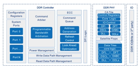
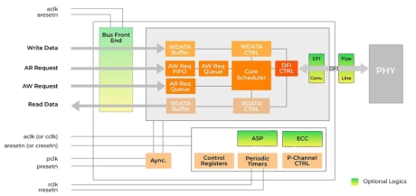
DDR and LPDDR 5/4/3/2 controllers for low power and high Reliability, Availability and Serviceability (RAS)
- Four memory controller offerings: uMCTL2: multi-ported memory controller supporting JEDEC standard DDR2, DDR3, DDR4, LPDDR, LPDDR2, LPDDR3, and LPDDR4, and LPDDR4X SDRAM and DIMM modules
- uPCTL2: Single-ported version of uMCTL2 with no internal scheduler; DDR5/4 controller: multi-ported memory controller supporting JEDEC standard DDR5, DDR4 SDRAMs and DIMM modules
- LPDDR5/4/4X controller: multi-ported memory controller supporting JEDEC standard LPDDR5, LPDDR4, and LPDDR4X SDRAMs
- High-bandwidth design with up to 64 CAM entries for Reads and 64 CAM entries for Writes, and latency as low as 6 clock cycles
-
DDR and LPDDR 5/4/3/2 controllers for low power and high Reliability, Availability and Serviceability (RAS) targeting automotive
- Four memory controller offerings: uMCTL2: multi-ported memory controller supporting JEDEC standard DDR2, DDR3, DDR4, LPDDR, LPDDR2, LPDDR3, and LPDDR4, and LPDDR4X SDRAM and DIMM modules
- uPCTL2: Single-ported version of uMCTL2 with no internal scheduler; DDR5/4 controller: multi-ported memory controller supporting JEDEC standard DDR5, DDR4 SDRAMs and DIMM modules
- LPDDR5/4/4X controller: multi-ported memory controller supporting JEDEC standard LPDDR5, LPDDR4, and LPDDR4X SDRAMs
- High-bandwidth design with up to 64 CAM entries for Reads and 64 CAM entries for Writes, and latency as low as 6 clock cycles
-
High Performance DDR 3/2 Memory Controller IP
- Supports DDR3/DDR2 SDRAM
- 16 bits width DDR2/DDR3 SDRAM Interface
- Memory Clock up to 462MHz, DFI Clock up to 462MHz
- Support DDR2 667/800/1066 and DDR3 667/800/1066/1333/1600/1866
-
DDR 4/3 Memory Controller IP - 2400MHz
- Support s DDR 4 /DDR3 SDRAM
- 16 bit s width , Single Channel DDR 4 /DDR3 SDRAM Interface .
- 16 bits for per channel, could support 2 x8 bits DDR3, but could not support 2 x8 bits DDR4.
- Memory Clock up to 6 66 MHz, DFI Clock up to 666 MHz .
-
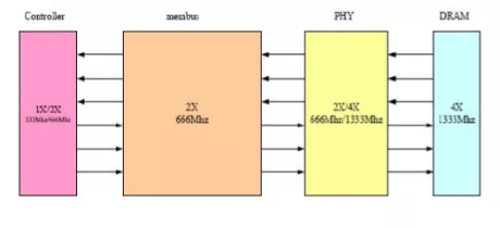
High Speed DDR Interface Solution
- Brite provides a complete DDR subsystem including not only controller, PHY and IO, but also corresponding tuning and configuration software. And this solution can support LPDDR2, DDR3, LPDDR3, DDR4 and LPDDR4/4x combo PHY with the data rate from 667Mbps to 4266Mbps.
-
-
DDR3/ DDR3L Combo PHY IP - 1600Mbps (Silicon Proven in UMC 40LP)
- Interface: SSTL
- Maximum controller clock frequency of 400MHz resulting in maximum DRAM data rate of 1600Mbps
- Data path width scales in 8-bit increment
- Programmable output impedance
-
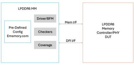
Simulation VIP for LPDDR6
- This Verification IP (VIP) is intended for modeling the upcoming JEDEC Low-Power Memory Device, LPDDR6 design specification.
- It provides a mature, highly capable compliance verification solution that supports simulation, formal analysis, and hardware acceleration platforms, making it applicable to intellectual property (IP), system-on-chip (SoC), and system-level verification.