DDR5 Controller IP
Welcome to the ultimate DDR5 Controller IP hub! Explore our vast directory of DDR5 Controller IP
All offers in
DDR5 Controller IP
Filter
Compare
52
DDR5 Controller IP
from
15
vendors
(1
-
10)
-
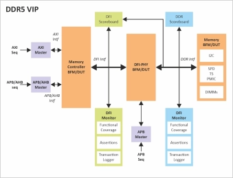
DDR5 LRRDIMM Verification IP
- Compliant to JEDEC DDR5 SDRAM Specification, Data Buffer & RCD Specification.
- Supports connection to any DDR5 Memory Controller IP communicating with a JEDEC compliant DDR5 Memory Model.
- Supports configurable SDRAM addressing of different sizes (x4, x8 and x16).
- Available in all memory sizes up to 64 Gb.
- Supports for all speed-grades/speed-bins.
-
DDR5 RDIMM Verification IP
- The DDR5 RDIMM Verification IP provides an effective & efficient way to verify the components interfacing with DDR5 RDIMM interface of an ASIC/FPGA or SoC.
- The DDR5 RDIMM VIP is fully compliant with Standard DDR5 specification from JEDEC.
- This VIP is a light weight with an easy plug-and-play interface so that there is no hit on the design time and the simulation time.

-
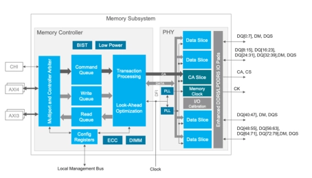
DDR5 MRDIMM PHY and Controller
- The DDR5 12.8Gbps MRDIMM Gen2 PHY and controller memory IP system solutions double the performance of DDR5 DRAM.
- The DDDR5 12.8Gbps design and architecture address the need for greater memory bandwidth to accommodate unprecedented AI processing demands in enterprise and data center applications, including AI in the cloud.
-
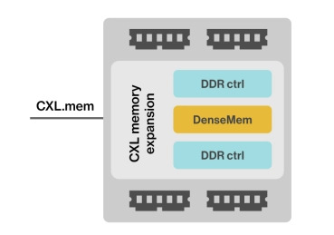
CXL memory expansion
- Turn key solution: compression, compaction, memory management
- Automatic compressed memory tier
- Multi-instance support to match interface throughput
- Cache line granularity decompression for highest read performance (proprietary algorithm)
-
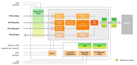
MRDIMM DDR5 & DDR5/4 PHY & Controller
- The DDR IP Mixed-Signal MRDIMM DDR5 PHY and DDR5/4 Combo PHY provide turnkey physical interface solutions for ICs requiring access to JEDEC compatible SDRAM or MRDIMM/ RDIMM/ LRDIMM/ UDIMM DDR5 devices
- It is optimized for low-power and high-speed applications with robust timing and small silicon area
- It supports all JEDEC DDR5/4 SDRAM components in the market

-
-
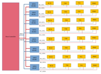
DDR5 Serial Presence Detect (SPD) Hub Interface
- The SPD5 Hub Function IP has been developed to interface I3C/I2C Host Bus and it allows an isolation of local devices like Temperature Sensor(TS), from master host bus
- This SPD5 has Two wire serial interface like SCL, SDA
-
DDR5 REGISTERING CLOCK DRIVER (RCD) IP - (DDR5RCD03)
- The DDR5RCD03 is a registering clock driver used on DDR5 RDIMMs and LRDIMMs
- Its primary function is to buffer the Command/Address (CA) bus, chip selects, and clock between the host controller and the DRAMs
- It also creates a BCOM bus which controls the data buffers for LRDIMMs

-
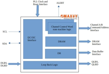
DDR5 REGISTERING CLOCK DRIVER (RCD) IP - (DDR5RCD01)
- The DDR5RCD01 is a registering clock driver used on DDR5 RDIMMs and LRDIMMs
- Its primary function is to buffer the Command/Address (CA) bus, chip selects, and clock between the host controller and the DRAMs
- It also creates a BCOM bus which controls the data buffers for LRDIMMs
-
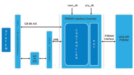
AP Memory UHS PSRAM Controller
- This controller supports AP Memory’s UHS series of high speed PSRAM devices which can clock frequencies of upto 1066 MHz.
- This controller enables smooth integration of APMemory’s UHS OPI PSRAM memory device chips into various new-gen devices made with mobile and wearable low power SoCs’.
- This memory controller implementation is designed to give the user full flexibility for driving the memory control signals and timing adjustment for data sampling.
