Memory Controller/PHY IP for GLOBALFOUNDRIES
Welcome to the ultimate
Memory Controller/PHY IP
for
GLOBALFOUNDRIES
hub! Explore our vast directory of
Memory Controller/PHY IP
for
GLOBALFOUNDRIES
All offers in
Memory Controller/PHY IP
for
GLOBALFOUNDRIES
Filter
Compare
21
Memory Controller/PHY IP
for
GLOBALFOUNDRIES
from
6
vendors
(1
-
10)
-
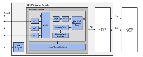
LPDDR5T / LPDDR5X / LPDDR5 Controller
- Support for all LPDDR5T/5X/5 devices
- Bank management logic monitors status of each bank
- Queue-based user interface with reordering scheduler
- Look-ahead activate, precharge, and auto-precharge logic
- Parity protection for all stored control registers
- PHY interface based on DFI 5.1 standard
-
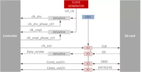
SD/EMMC PHY
- Include 1 clock, 1 bi-directional CMD, and 4 bi-directional DATA channel
- Design in GLOBALFOUNDRIES 22nm FDX process
- Data rate range: 50M~104MB/s
- Supports up to 208MHz clock
-
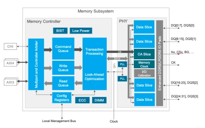
DDR PHY
- DDR5/4/3 training with write-leveling and data-eye training
- Optional clock gating available for low-power control
- Internal and external datapath loop-back modes
- I/O pads with impedance calibration logic and data retention capability
- Programmable per-bit (PVT compensated) deskew on read and write datapaths
- RX and TX equalization for heavily loaded systems
-
SD/eMMC - GlobalFoundries 12LP, North/South Poly Orientation
- Compliant with eMMC 5.1 HS400, SD 6.0 SDR104, DDR50, JESD8-7a (1.2V/1.8V) and JESD8c.01 (3.3V)
- Fully integrated hard macro with high speed IOs and DLL/delay lines
- Fine resolution DLL/delay lines for HS400 strobe and HS200/SDR104 auto-tuning
- Easy to integrate with the highly optimized Synopsys SD/eMMC Host Controller IP, providing a complete low risk solution
-
LPDDR5/4/4X PHY - GF 12LP+ for Automotive ASIL B Random, AEC-Q100 Grade 1
- Supports JEDEC standard LPDDR5X, LPDDR5, LPDDR4 and LPDDR4X SDRAMs
- Support for data rates up to 6400 Mbps
- Designed for rapid integration with Synopsys’ LPDDR5/4/4X controller for a complete DDR interface solution
- DFI 5.0 controller interface

-
LPDDR5/4/4X PHY - GF 12LP+
- Supports JEDEC standard LPDDR5X, LPDDR5, LPDDR4 and LPDDR4X SDRAMs
- Support for data rates up to 6400 Mbps
- Designed for rapid integration with Synopsys’ LPDDR5/4/4X controller for a complete DDR interface solution
- DFI 5.0 controller interface

-
DDR5/4 PHY - GF 12LP+
- Supports JEDEC standard DDR5 and DDR4 SDRAMs
- High-performance DDR PHY supporting data rates up to 8400 Mbps
- PHY independent, firmware-based training using an embedded calibration processor
- Supports up to 4 trained states/ frequencies with <3μs switching time

-
DDR multi PHY
- Compatible with JEDEC standard DDR2/DDR3/LPDDR (or Mobile DDR)/ /LPDDR2/LPDDR3 SDRAMs
- Operating range of 100MHz (200Mb/s) to 533MHz(1066Mb/s) in DDR2/DDR3/LPDDR2/LPDDR3 modes
- Operating range of DC to 200MHz in Mobile DDR mode
- PHY Utility Block (PUBL) component
-
GDDR6 PHY IP on GF 12nm LPP
- The UniIC GDDR6 PHY,subsequently referred to as the UNIIC_GD6PHY, is designed for performance and power efficiency, its target is to deliver industry-leading data rates of up to 12Gbps/13Gbps/14Gbps and is compatible with JEDEC standard JEDEC250 and DFI 3.1
- The UNIIC_GD6PHY is used to transfer the Command/Address and Datas between the memory controller and the GDDR6 DRAM device; _x000D_ The UNIIC_GD6PHY is available in Global Foundries FinFET 12LPP technology
- The UNIIC_GD6PHY is fully documented and comes with a comprehensive set of deliverables for ease of system modeling and integration.
-
SATA 6G PHY in GF (40nm, 28nm)
- Compliant with SATA/eSATA v3.3, AHCI v1.3 and SATA PIPE v4.3 specifications
- AMBA 2.0 AHB and AMBA 3 AXI subsystem interfaces
- AMBA 4 AXI and ACE-Lite bus interfaces
- Memory data protection and memory address parity protection