SD/EMMC PHY
The SD/EMMC PHY IP supports up to 208MHz which compliant with SDIO and EMMC specification.
Overview
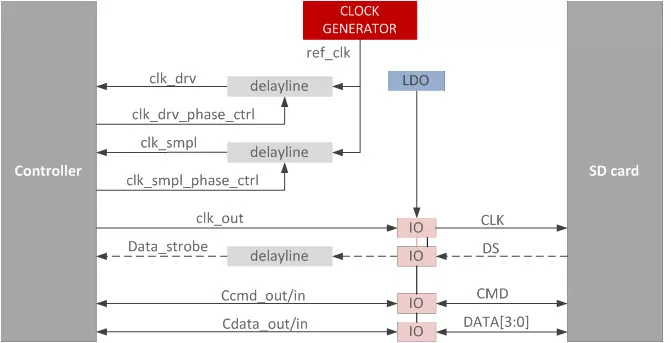
The SD/EMMC PHY IP supports up to 208MHz which compliant with SDIO and EMMC specification. The SDIO/EMMC PHY includes DLL/Delay lines and IO. I/O input voltage is 3.3V, and signal voltage is within 3.3V/1.8V. Delay line supports dual data rate for DDR50, and single data rate for SDR104.
The DLL/Delay lines in SD/EMMC PHY IP support fine resolution, and the IP support bypass mode to control the delay lines.
Key features
- Include 1 clock, 1 bi-directional CMD, and 4 bi-directional DATA channel
- Design in GLOBALFOUNDRIES 22nm FDX process
- Data rate range: 50M~104MB/s
- Supports up to 208MHz clock
- Signal voltage supports 3.3/1.8V
- IO driver supports 33/50/66/100Ω terminations, and default is 50Ω
- Include high speed IOs and DLL/Delay lines
- DLL/Delay lines support fine resolution
- Core area: 62628.5um^2 (not include IO)
- Power consumption:
- 9mW@200MHz/signal voltage 1.8V
Block Diagram

Specifications
Identity
Files
Note: some files may require an NDA depending on provider policy.
Provider
Learn more about Single-Protocol PHY IP core
Design IP Faster: Introducing the C~ High-Level Language
Universal Flash Storage: Mobilize Your Data
Can MIPI and MDDI Co-Exist?
Enter the Inner Sanctum of RapidIO: Part 1
Networking software key to PICMG 2.16 optimization
Frequently asked questions about Single-Protocol PHY IP
What is SD/EMMC PHY?
SD/EMMC PHY is a Single-Protocol PHY IP core from VeriSilicon Microelectronics (Shanghai) Co., Ltd. listed on Semi IP Hub.
How should engineers evaluate this Single-Protocol PHY?
Engineers should review the overview, key features, supported foundries and nodes, maturity, deliverables, and provider information before shortlisting this Single-Protocol PHY IP.
Can this semiconductor IP be compared with similar products?
Yes. Buyers can compare this product with similar semiconductor IP cores or IP families based on category, provider, process options, and structured technical specifications.