ggNMOS (grounded-gated NMOS)
By Sofics
ggNMOS intro:
For decades, a traditional workhorse device for ESD protection for standard applications in CMOS technology has been the grounded-gate NMOS device (ggNMOS).
Nevertheless, we have been explaining the operation of this device countless times, including as recently as 3 weeks ago. So, it is time for a short blog article. The schematic of a ggNMOS and its typical ESD I-V characteristic are sketched in Figure 1.a and b.
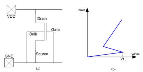
Figure 1: Figure 1: ggNMOS schematic (a), and the ggNMOS IV characteristic (b).
How does NMOS snapback work?
To understand the physical operation, one should study the silicon cross-section of the NMOS (simplified in Figure 2.a), and consider the equivalent bipolar schematic that one can uncover (Figure 2.b).
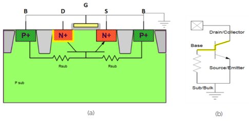
Figure 2: NMOS cross-section (a) and the equivalent bipolar schematic (b).
When increasing the drain/collector voltage versus the grounded source/emitter/bulk a reverse voltage will build up across the drain to the substrate junction in Figure 2.a, which is also the collector/base diode in Figure 2.b. Until that diode breaks down (assuming no punch-through occurs) there will be no current flowing through the reverse diode or junction. At some point, the reverse diode will breakdown and current will flow in the depletion region of the diode. Carriers will be accelerated in the electric field and create an avalanche effect when knocking into other fixed carriers. This is illustrated in Figures 3 a and b. As the reverse voltage is increasing, the current will increase rapidly.
To read the full article, click here
Related Semiconductor IP
- ReRAM NVM in DB HiTek 130nm BCD
- UFS 5.0 Host Controller IP
- PDM Receiver/PDM-to-PCM Converter
- Voltage and Temperature Sensor with integrated ADC - GlobalFoundries® 22FDX®
- 8MHz / 40MHz Pierce Oscillator - X-FAB XT018-0.18µm
Related Articles
Latest Articles
- An FPGA-Based SoC Architecture with a RISC-V Controller for Energy-Efficient Temporal-Coding Spiking Neural Networks
- Enabling RISC-V Vector Code Generation in MLIR through Custom xDSL Lowerings
- A Scalable Open-Source QEC System with Sub-Microsecond Decoding-Feedback Latency
- SNAP-V: A RISC-V SoC with Configurable Neuromorphic Acceleration for Small-Scale Spiking Neural Networks
- An FPGA Implementation of Displacement Vector Search for Intra Pattern Copy in JPEG XS