Variable-integration-time image sensor for wide dynamic range
by Takaya Yasuda, Takahiro Ogi, Takayuki Hamamoto, Tokyo University of Science
Kiyoharu Aizawa, University of Tokyo
Tokyo Japan
Abstract
An image sensor for wide dynamic range by adapting integration time of each pixel is proposed. The integration time of each pixel is selected among several lengths of integration time and the integration time is shortened if the pixel is bright. Although the integration time of each pixel varies, the pixel intensity is adjusted on the sensor in real time. The dynamic range of the pixel value output from the proposed sensor is much widened. A prototype of 64×48 pixels has been fabricated. The proposed sensor has simple functions for detection of saturation to control the integration time and nonlinear image reconstruction. By experiments, it has been verified that the sensor can achieve wide dynamic range by adapting to light.
1. Introduction
We have been investigating novel smart sensors in which every pixel independently controls its integration time[1-3]. The integration time is controlled so that it has higher temporal resolution or wider dynamic range.
A CCD sensor with electronic shutter is capable of imaging at variable integration time[4]. However, the integration time is constant for all pixels and individual variation is not possible. Therefore it cannot enhance intrascene dynamic range.
The some methods of multiple-readout scheme with some different integration times have been proposed[5,6]. The multiple intensities from a single pixel are combined to improve the intrascene dynamic range. We have fabricated two adaptive integration time image sensors [1,2]. In two prototypes, the integration time for each pixel is adapted to motion and light intensity. They can reduce image blur as well as improving the intrascene dynamic range. Although such methods which use different integration time can extend the intrascene dynamic range, most of them, including our previous two sensors, require the external memory or the external processing circuits for image reconstruction.
In this paper, we describe a new variable-integration-time image sensor based on a column parallel architecture. It has 64×48 pixels. In this new prototype, integration time of each pixel is controlled by detecting saturation, and a real time processing circuit for image reconstruction is integrated on the sensor chip.
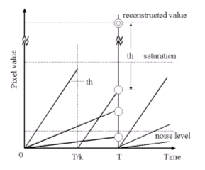
Fig.1 Integration process of pixel values. (the number of the comparison to threshold is one)
2. Method for extending dynamic range
2.1 Integration-time control for each pixel
We use the intermediate pixel values of each pixel to extend dynamic range. Fig.1 shows an example of an integrating pixel value based on our proposal. As a conventional image sensor, all pixel values are output once at the fixed interval (T). T is the maximum integration time and frame rate is decided by 1/T. At the intermediate of integration(T/k), the photodiode (PD) value is compared to a threshold (th) and the saturation is detected when PD value exceeds the threshold. If saturation is detected, the PD value is selectively reset. Therefore, the integration time of a bright pixel is shorter than that of the other pixel. Because of the variable integration time, the pixel intensity needs to be reconstructed later. We can control both comparison timing (k) and threshold (th). Because the comparison to the threshold is very simple, the high frame operation can be done by a small circuit on an image sensor.
2.2 Relationship between incident light and pixel value
Fig.2 shows the I/O characteristic when the number of the comparison to the threshold is one (k=3/2, th=88). The dynamic range of our proposal is extended compared to the conventional sensor. We can adjust the characteristic by changing k(comparison timing) and th(threshold) freely. The slope of line B is determined by 1-1/k and the cross point between line A and line B also depends on k and th.
If the comparison-reset operation is done during integration repeatedly, the dynamic range is much wider. Fig.3 shows the I/O characteristic when the number of the comparison to threshold is three (k1=4, th1=25: k2=2, th2=50: k3=30/29, th3=147). During integration, the PD value is compared to one of three different thresholds (th1,th2,th3) at three different timing (k1,k2,k3). Only when the PD value exceeds the threshold, the PD value is reset and a flag signal is stored in a memory. At the end of the integration, the reconstruction circuit could add the thresholds to the final PD value when the corresponding flag signals are high. In Fig.3 the slopes of lines A,B,C and D are 1,1-1/k1,1-1/k2,1-1/k3 and the cross points of each two lines are described in next equation.
![]()
2.3 Condition of parameters for saturation detection
When the number of saturation detection during integration is n, some conditions are necessary to keep continuity of the characteristic between light intensity and pixel value. If a pixel is not detected as saturated once, the pixel must not be detected as saturated at the following timing.
[1] If the saturation detection is done at T/ki (i=1,2,3,?cn),

T is maximum length of integration time. Vs is maximum intensity of input light.
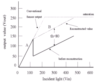
Fig.2 I/O characteristic when the number of the comparison to threshold is one (k=3/2,th=88).
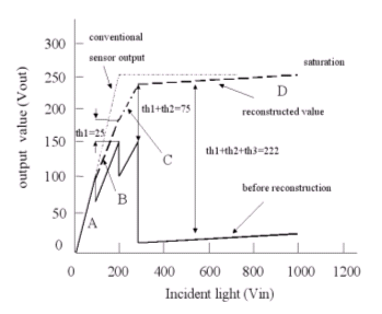
Fig.3 I/O characteristic when the number of the comparison to threshold is three (k‚P=4,th‚P=25: k2=2, th2=50: k3=30/29, th3=147).
[2] If the threshold of saturation detection is thi (i=1,2,3,?cn), th1<th2<?c<thn.

2.4 Linear reconstruction by external circuits
Although the reconstruction on the sensor is nonlinear, the linear reconstruction can be done by using raw PD output and flag signals if the linear pixel value is required for post processing. In Figs. 2 and 3, the slope of the lines without reconstruction is represented by the equation
![]()
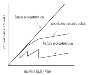
Fig.4 Linear reconstruction.
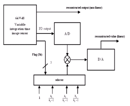
Fig.5 Peripheral circuits for linear reconstruction.
Fig.4 shows the I/O characteristic of nonlinear and linear reconstruction. By multiplying the PD value and the invert value of the slope, we can reconstruct the pixel value linearly. Fig.5 shows the external circuits for the real-time linear reconstruction. It consists of the circuits for A/D, D/A, multiplier and selector of the thresholds. The circuits except A/D and D/A can be implemented on a field-gate programmable array (FPGA) chip.
2.5 Computer simulation of the still image
Fig.6 shows the results of computer simulation by CCD images sensor. We use the several still images which are obtained with the different integration time. Fig.6 (a) shows the image with longest integration time which corresponds to the conventional output image. Figs.6 (b) and (c) are the reconstructed images when the number of the comparison to threshold is three. Table 1 shows their parameters which are determined experimentally. The nonlinear reconstruction is performed on the sensor by adding the threshold to the PD value. On the other hand, the linear reconstruction requires the external circuits to normalize the PD value with length of integration time.
Table 1 Parameters of the comparison for simulation of still images.
| Detection NO | k | th |
| 1 | 4 | 25 |
| 2 | 2 | 50 |
| 3 | 3/2 | 150 |
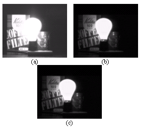
Fig.6 Simulation results of still images by using CCD sensors. (a) Conventional output image, (b) Proposed output image by nonlinear reconstruction, (c) Proposed output image by linear reconstruction.
Although the center of the conventional image is saturated, the characters written in the peripheral part of a light bulb are much clear in the case of the proposed images. It appears that the proposed method can widen the intrascene dynamic range regardless of
linear or nonlinear reconstruction.
2.6 Computer simulation of moving images
Fig.7 shows the results of computer simulation for moving images. Table 2 shows their parameters which are determined experimentally. Figs.7 (a) and (b) show the images which correspond to the conventional output image. Figs.7 (c) and (d) are the reconstructed images when the number of the comparison to threshold is three. We can distinguish the characters written on the periphery of the light bulb. In this simulation, motion blur of the proposed images is reduced because of short integration time for bright pixels.
Table 2 Parameters of the comparison for simulation of moving images
| Detection No | ‚‹ | th |
| 1 | 4 | 25 |
| 2 | 2 | 50 |
| 3 | 3/2 | 150 |
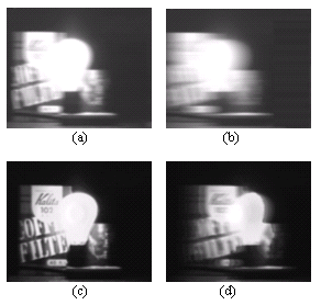
Fig.7 Simulation results of the moving image by using CCD sensor. (a) Conventional output image; speed is 30 pixels/frame. (b) Conventional output image; speed is 100 pixels/frame. (c) Proposed output image by nonlinear reconstruction; speed is 30 pixels/frame. (d) Proposed output image by nonlinear reconstruction; speed is 100 pixels/frame.
3. Design of variable-integration-time image sensor
Fig.8 shows the processing scheme in each pixel of the variable-integration-time image sensor. It has processing circuits for the comparison to threshold and real time reconstruction, and 3 bit memory. The maximum number of the comparison to threshold during a frame is three. The integrating PD value is compared to one of three different thresholds Vth1, Vth2 and Vth3.
When the PD value exceeds the threshold, the PD value is reset and 1 bit flag signal is stored in the memory. When the integration is finished, the reconstruction circuit could add the corresponding thresholds to the final PD value for nonlinear reconstruction. Each PD value is reset when the integration is finished or the intermediate PD value exceeds the threshold, therefore, the integration time is different pixel by pixel. We can control the threshold voltages and the timing for the comparison to the thresholds freely.
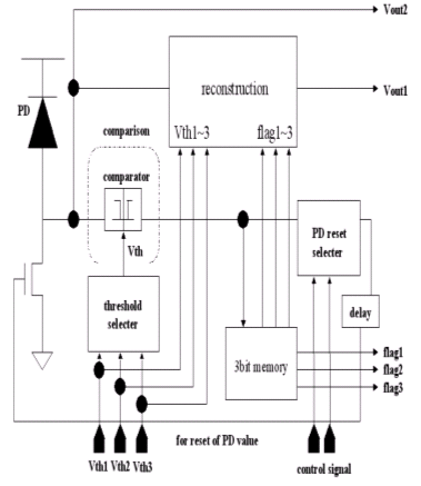
Fig.8 Processing scheme of a pixel.
Fig.9 shows the block diagram of the variable-integration-time image sensor. In order to share the processing circuits among the pixels in a column, it makes use of a column parallel architecture. This sensor is divided into transducer, memory and processing elements. Using two vertical shift registers, the pixels and the memories are scanned line by line, therefore minimum integration time is determined by the length of processing time for each row. The proposed sensor has a horizontal shift register for outputting reconstructed pixel value, raw pixel value and 3 bit flag signals.
4. Experiments
4.1 Prototype chip
We fabricated the new variable-integration-time image sensor by using 2-poly 2-metal 0.8ƒÊm CMOS process. Fig.10 shows the layout of the prototype. The test circuits are also implemented on the same chip. The outline of the prototype is listed in Table 3. Dynamic range can be extended from 53.9dB to 107.6dB. Because the CDS circuit is not implemented on this prototype, the fixed pattern noise between columns is 2.43mVrms. Maximum frame rate is estimated about 1400fps.
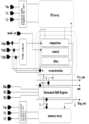
Fig.9 Block diagram.
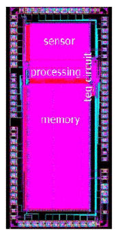
Fig.10 Layout of the prototype chip.
Table 3 Outline of the prototype.
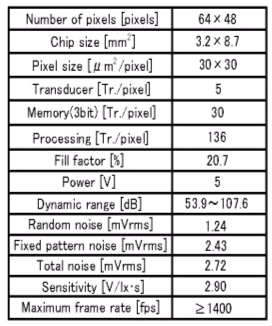
Table4 Parameters of the comparison for experiment of still images.
| Detection No | K | th [V] |
| 1 | 16 | 5.24 |
| 2 | 4 | 3.34 |
| 3 | 2 | 3.24 |
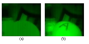
Fig.11 Still images obtained by the prototype. (a) Conventional output image. (b) Nonlinear output image reconstructed by the on-sensor circuit.
4.2 Still images obtained by the prototype
Fig.11 shows the example images obtained by the prototype chip. Fig.(a) is the conventional image and (b) is the nonlinear reconstructed image with three comparisons. Table 4 shows the parameters of the comparison which are determined experimentally. In Fig.(b), "A" written on the electric bulb is shown because of extending dynamic range.
4.3 Moving images obtained by the prototype
Fig.12 shows the moving images obtained by the prototype chip. Fig.(a) is the conventional output images and Fig.(b) is the output image reconstructed by external circuits linearly. Table 5 shows the parameters of the comparison which are determined experimentally. Character "A" written on the electric bulb can not be recognized in Fig12.(a) but be shown in Fig.(b).
Table 5 Parameters of the comparison for experiment of moving images.
| Detection NO | K | th[V] |
| 1 | 16 | 2.581 |
| 2 | 4 | 2.123 |
| 3 | 2 | 1.889 |
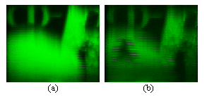
Fig.12 Moving images obtained by the prototype. (a) Conventional output images. (b) Output images by linear reconstruction.
5. Conclusion
In this paper, we introduce new variable-integration-time image sensor. The proposed sensor has the circuits for controlling integration time pixel by pixel and reconstructing the pixel value nonlinearly. The linear reconstruction can be done by the external circuit using FPGA.
By experiments, it has been verified that the sensor can achieve wide dynamic range by controlling integration time.
References
[1] T.Hamamoto, K.Aizawa, M.Hatori, ?gMotion adaptive image sensor?h, Proc. of IEEE Workshop on CCD and advanced Image Sensors, R30, 1997.
[2] T.Hamamoto, K.Aizawa, ?gA computational image sensor with adaptive pixel-based integration time?h, IEEE trans. On Solid-State Circuits, Vol.36, No.4, pp.580-585, April, 2001.
[3] T.Yasuda, T.Hamamoto, K.Aizawa, ?gAdaptive integration time image sensor with real time reconstruction function?h, IEEE trans. on Electron Devices Vol.50, No.1, pp.111-120, 2003
[4]F.Ando, ?gMulti-functional Solid State Imaging Techniques?h, ITEJ, Vol.44, No.2, pp. 127-131, 1990.
[5]O.Shrey, J.Huppertz, G.Filimonovic, A.BuBmann, W.Brockherde and B.J.Hosticka, ?gA 1k times 1k High Dynamic Range CMOS Image Sensor with On-Chip
Programmable Region of Interest Readout?h, Proc. of European SolidState Circuits Conference, pp.124-127, Sept., 2001.
[6] O.Yadid-Pecht and E.Fossum, ?gWide intrascene dynamic range CMOS APS using dual sampling,?h IEEE Trans. Electron Devices, vol. 44, pp.1721-1723, Oct. 1997.
Related Semiconductor IP
- NPU IP Core for Mobile
- NPU IP Core for Edge
- Specialized Video Processing NPU IP
- HYPERBUS™ Memory Controller
- AV1 Video Encoder IP
Related White Papers
- From a Lossless (~1.5:1) Compression Algorithm for Llama2 7B Weights to Variable Precision, Variable Range, Compressed Numeric Data Types for CNNs and LLMs
- Reducing Time To Market for System On Chip Using IP Development and Integration Flow
- New Applications Areas Driving Higher Dynamic Range Converters
- Stretching the Dynamic Range of ADCs - A case study
Latest White Papers
- Ramping Up Open-Source RISC-V Cores: Assessing the Energy Efficiency of Superscalar, Out-of-Order Execution
- Transition Fixes in 3nm Multi-Voltage SoC Design
- CXL Topology-Aware and Expander-Driven Prefetching: Unlocking SSD Performance
- Breaking the Memory Bandwidth Boundary. GDDR7 IP Design Challenges & Solutions
- Automating NoC Design to Tackle Rising SoC Complexity