Understanding the reuse of a DSP architecture for different designs (Ceva)
As DSP usage becomes ubiquitous for voice compression and decompression, audio decoding and encoding applications, signal modulators and equalizers, video applications, and advanced vocoders and transcoders, the market need for DSPs is tremendous and growing. These different applications have created a wide range of processing demands, and have driven DSP specialists to customize their offerings and provide their customers with DSP technologies that can better perform specific tasks or applications.
These application-specific programmable DSPs, though cost effective per specific application, are not competitive platforms for use with other tasks and functions. As a consequence, OEMs often tend to switch DSP architectures for different applications, and migrate to a new architecture for the benefit of next generation products.
This DSP architecture framework meets the varied requirements imposed by different users and offers diverse benefits to different DSP users and applications.
Investment in DSP technology
A DSP technology is not utilized in a void; rather it is part of an integrated system, a total solution. Assuming an IP DSP core is in place, it must be integrated into a System on a Chip (SoC), with a set of peripherals, memories, system interfaces, etc. Some of these can be easily reused for a newer DSP core, by running on standard bus connectivity, while others require a redesign, sometimes from scratch. For example, a memory controller is dependent on the specific processor, and it differs from one processor to the other. Such a memory controller can include sophisticated multi-channel DMAs, a cache controller, and a memory management unit (MMU). Other tightly coupled peripherals and accelerators require a design from scratch when switching DSP architecture, because they interface with the DSP in a very distinct manner.
Porting software is also a major development task to be carefully monitored. A DSP already deployed by a company has all the SW components installed in place. Developing the entire SW framework for a new DSP architecture is a long and laborious task, even with a highly optimized C-compiler. Another investment related to SW porting is the process of learning the SW development tools (SDT) that complement the DSP. The knowledge of the Integrated Development Environment (IDE) in general and of the compiler optimization techniques in particular should be rebuilt when switching DSP architecture, with minimum reusability.
With demands for performance, speed and low power consumption now being drawn as increasingly small circles, switching to a completely new DSP architecture is a frequent, and costly, occurrence. DSP technology reuse could reduce, if not eliminate, the additional costs and efforts required when planning and designing the next generation application, mitigating the above-mentioned re-investments when adopting a new DSP.

Fig. 1
DSP technology te-use
As competition drives the industry to produce new solutions, corporations are trying to leverage the technologies behind their current products for next generation products and applications. With high development and verification costs, if a company has large investments in a particular DSP technology for a specific product, why not exploit this for the next generation product? Moreover, why not reuse the same DSP for an entirely different application?
Take a large semiconductor conglomerate, developing and manufacturing different products and appliances, from wireless handsets to home entertainment devices. Imagine the cost effectiveness of reusing the same DSP platform to fit different products. Imagine the explosion of possibilities if the conglomerate can share DSP platforms among different products and through different generations. Could a single investment in DSP technology be leveraged and reused across different product lines?
DSP technology reuse is influenced by the level of programmability. A fully programmable solution that minimizes the usage of hardwired blocks offers the ability to create a single chip that addresses multiple applications, simply by updating the SW. This is pertinent also for low-end applications trying to go for the final cost reduction phase. Even extremely costsensitive applications, such as portable audio players, prefer the usage of a programmable DSP.
Such an approach eliminates the need (and associated cost) for additional silicon spins for new product derivatives and provides a flexible and upgradeable solution that supports multiple audio codecs.
The trend towards SW programmable DSPs is evident given the ever-changing standards of telecom, broadband and multimedia markets, and the exponentially increasing cost of silicon re-spin in 0.13u technologies and beyond. Both issues can be addressed by utilizing the same DSP platform (and in some cases, the same chip) for next generation products.
For DSP technology to be easily reused, a modular and flexible design should be created. The DSP HW subsystem should be made of building blocks and configurable interconnectivity, allowing re-spinning new silicon for a different application in a matter of weeks. By using a modular design, the same DSP architecture can be effortlessly complemented with the appropriate system components. The DSP SW modules can communicate using a uniform API protocol. An application builder utility can save months of integration effort, bringing all the SW pieces together, including SW modules, task scheduler, OS and inter-processor communication.

Fig. 2
Architecture reuse
One possible solution for reducing DSP switching costs is to offer a powerful general purpose DSP that could fit into many different applications. This can enable the customer to commit to a single DSP architecture and reuse it for different products.
The disadvantage of this concept is the level of suitability of such a processor to different requirements. It obviously cannot be optimized for diverse and sometimes even conflicting constraints.
A more innovative solution is in the form of an architecture framework. This new concept is based on a single architecture, out of which multiple DSP designs can be extracted. Each DSP design can fit a different market with varying processing requirements and different operational points, in terms of speed, power consumption and die size.
The architecture learning curve, including the SW development tools, the system I/F and peripherals can be reused across all DSP designs. Such architecture enables the reuse of any SW components previously developed for a new DSP design in the same architecture framework.
The pioneering CEVA-X DSP Architecture is based on the concept of such an architecture framework. This framework is comprehensive enough in order to support various processing demands, from a 2 MAC DSP design up to 8 MAC DSP. The core can either process 16- bit or 32-bit native data word sizes.
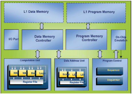
The level of parallelism supported is also variable, as well as the memory subsystem structure and the system I/F. Figure 1 shows a block diagram of the CEVA-X1620 DSP, a 16-bit dual MAC implementation derived from the CEVA-X architecture.
Another important feature of DSPs today is the ability to extend the instruction set according to new standards requirements.
A base architecture is fixed in place, while new instructions and their related HW can be customized ensuring that such a DSP will continue to serve the needs of new forthcoming algorithms.
This flexibility has some cost associated with it. From the architecture point of view, the DSP has to dedicate some of its encoding space for such future extensions. The outcome is a smaller encoding space for the base instruction set architecture, and more limited computational capabilities.
Other sacrifices of an extendible architecture are dedicated ports to the register files and other indications, not utilized by the non-extended DSP designs. From the SW development tools point of view, an extendible DSP requires high level of flexibility.
User-defined instructions need to be supported by the full tool chain, including the compiler, simulators and code generation tools.
Table 1 suggests different DSP designs based on the CEVA-X architecture framework, each matching a specific market segment.

Bit stream unpacking
All CEVA-X DSP family members are accompanied by the necessary HW and SW frameworks. This revolutionizing offering enables customers to quickly develop their application around the DSP while minimizing the associated risk and cost.
The HW open platform surrounding the CEVA-X DSPs is a scalable subsystem, comprising of a rich set of peripherals and configurable interconnectivity, which allows for further customization and differentiation.
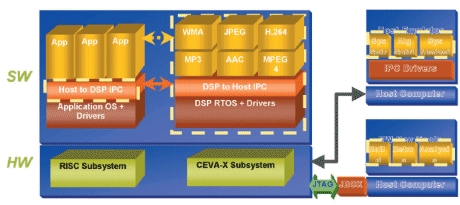
The SW open platform consists of a large set of SW libraries targeting different markets, an application builder composer for integrating the SW components, as well as a real-time OS and an inter-processor communication function. Figure 2 describes the functionality and interface of the SW open platform around the CEVA-X.
Providing this robust set of offerings ensures that even the same DSP from the CEVA-X family can be reused again and again for different applications, leveraging on previously invested design and development efforts.
The life cycle of a DSP is relatively short as companies are continuously moving to more powerful processors, with more computational capabilities and higher speeds. Switching from one DSP architecture to another entails a huge cost related to the learning curve associated with the HW, SW and system views of the DSP.
To break the cycle of buying and adopting a new DSP architecture for every new application or the ever increasing processing demands, a multi-purpose architecture framework is needed, which multiple DSP designs can cohabit, each DSP design addressing specific market needs.
Related Semiconductor IP
- NPU IP Core for Mobile
- MSP7-32 MACsec IP core for FPGA or ASIC
- NPU IP Core for Edge
- Specialized Video Processing NPU IP
- HYPERBUS™ Memory Controller
Related White Papers
- Why advanced DSPs running RTOSs are an ideal match for the IoT
- Paving the way for the next generation of audio codec for True Wireless Stereo (TWS) applications - PART 5 : Cutting time to market in a safe and timely manner
- eFPGA Saved Us Millions of Dollars. It Can Do the Same for You
- Understanding the Deployment of Deep Learning algorithms on Embedded Platforms
Latest White Papers
- Ramping Up Open-Source RISC-V Cores: Assessing the Energy Efficiency of Superscalar, Out-of-Order Execution
- Transition Fixes in 3nm Multi-Voltage SoC Design
- CXL Topology-Aware and Expander-Driven Prefetching: Unlocking SSD Performance
- Breaking the Memory Bandwidth Boundary. GDDR7 IP Design Challenges & Solutions
- Automating NoC Design to Tackle Rising SoC Complexity