Types of Memories in Computing System-On-Chips
Priyank Shukla, Director, Analog Mixed Signal Design, Insilicorp
Without even our consciously realizing, our life is touched by numerous computing systems. A computing system is essentially a system that can be instructed to carry out a set of arithmetic or logical operations automatically. As complex as it may sound, this abstract sounding definition can be a torchlight to define a computing system. Starting from the coffee machine that dispenses your favourite coffee or the traffic light that directs you to stop to the cell phone you hold are all examples of computing systems.
Arithmetic or logical operations in a computing system are executed in a processor or Central Processing Unit (CPU). Modern SoCs generally employ CPU cores from ARM, Intel or MIPS. A CPU processes digital information stored in forms of digital bits in some form of memory and generates results that are eventually stored in another memory location. So what types of memories are needed for a computing system? Let me try to answer this question with an analogy. Have you ever solved a complex math problem without a paper? Can you just arrive at the answer in one step? Maybe not, maybe that’s the reason you needed a piece of paper. If you are just interested only in the answer to a problem and not in the process, can you avoid/bypass the use of paper?
No! You need a paper to execute intermediate steps and arrive at the final answer. If you are only interested in the answer you can simply purge the page – this is precisely what a volatile memory does for a computing system – it gives the processor the memory to be used to arrive at the final outcomes. The final outcomes are ultimately stored in a non-volatile memory such as tapes/hard drives/ Solid State Drives that provide Non Volatile Memory (NVM). This article focuses on the types of volatile memories in modern SoCs.
The faster you can access the paper, the faster you would arrive at the answer, similarly, the faster an application processor access the volatile memory, the program will be executed faster. So a type of memory that can be accessed as fast as possible should be placed as close to the processor. That’s why modern-day processors integrate a type of volatile memory on chip and the memory is called cache. Most popular implementation allows Random Access to this Memory and thus such memory is called Random Access Memory or RAM. However, as it turns out all good things come at a price and so is the case with cache – it is expensive.
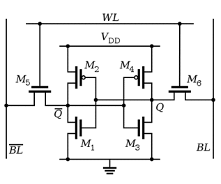
The basic cell to store one bit of information in these caches is called a 6-T cell, as it has six transistors connected in a way shown below

The voltage of the node holding the bit value does not change with time or in other words, remain static hence this implementation is called SRAM.
Another type of RAM, developed in the 1960s, is called DRAM (Dynamic Random-Access Memory) and offers a cheaper alternative to SRAM. However, this type of memory cannot be efficiently integrated on-chip with a processor and is always off-chip as a memory module. Most popular implementation of DRAM today provides data in both rising as well as falling edge of the clock and thus called DDR (Dual Data Rate) DRAM.
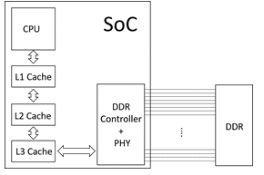
Modern computing SOCs integrates a number of processors and In order to optimize the performance of caches further the classes of caches in levels such as level 1, 2, 3 and so on and are called L1,L2, L3 caches. The below diagram shows a typical SoC computing system with three level of caches showing multiple processors as a single block of Central Processing Unit (CPU)

Whenever CPU needs to fetch digital information, it goes through levels of caches starting from L1 to L3 and if it doesn’t find the information there, it goes to a digital logic called memory controller or DDR controller for information. The memory controller then searches the information on off-chip DDR module. As depicted the above picture, a DDR PHY is needed to receive/transmit data off-chip.
Joint Electron Device Engineering Council (JEDEC) defines the specification for the DDR memory module and defines maximum data rate. In addition to serving memory requests from multiple processors, a DDR controller also addresses many other performances affecting features. This makes a memory controller significantly different from an interface controller (eg USB, PCIe or MIPI controller) as the implementation of former affects system performance significantly whereas the later simply implements a spec.

The way a DDR memory module is implemented, the memory bit cells, rows, columns need to be managed or controlled. In other words, a DDR memory module expects to be told which row and column should be read/written by the DDR controller. Since latency is one of the most critical specifications for memory systems and accessing a bit from same row or different row change latency significantly, the DDR controller plays a crucial role in system performance by maximizing row buffer hit rate.
By design, the time taken by DDR device to service a request from a bit cell is fixed, however, the DDR controller initiates parallelism by opening different groups of rows and columns (called rank and bank in DDR parlance) to maximize throughput overcoming implementation limitation.
Finally, as mentioned earlier DRAMs needs to be refreshed frequently to retain the stored value and the refresh rate depends on the process, voltage, and temperature, by changing the refresh rate intelligently, a DRAM controller can save power significantly.
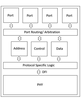
Instead of memory requests originating only from a processor, in some SoCs, a DDR controller might have to serve requests from GPU (Graphics processor) and other controllers as well. The below diagram shows an implementation of DDR interface in such a SoC, with each requester dealt with a dedicated port
The way a DDR controller interfaces multiple ports to a DDR device affects system performance significantly. Consider the operational case of a DDR controller in a mobile application processor SoC, it would get requests from GPU, main CPU, and other low-frequency CPUs as well. If the requests from GPU are buffered/delayed, the performance of mobile will be significantly reduced, however, there is a limit the requests from other ports can be delayed – the port arbitration/priority logic in the DDR controller is the secret sauce that balances this trade-off.
To summarise, on-chip SRAM cache, on-chip DRAM controller, and off-chip DDR device provide memory to a computing SoC. Considering the system architecture, it must be commented that the best memory performance is achieved by careful optimization of SRAM caches and DRAM device management through on-chip DDR controller.
Related Semiconductor IP
- NPU IP Core for Mobile
- NPU IP Core for Edge
- Specialized Video Processing NPU IP
- HYPERBUS™ Memory Controller
- AV1 Video Encoder IP
Related White Papers
- Types of Storages for Computing System-On-Chips
- Testing Of Repairable Embedded Memories in SoC: Approach and Challenges
- The rise of FPGA technology in High-Performance Computing
- New AI Computing in Consumer Electronics
Latest White Papers
- Transition Fixes in 3nm Multi-Voltage SoC Design
- CXL Topology-Aware and Expander-Driven Prefetching: Unlocking SSD Performance
- Breaking the Memory Bandwidth Boundary. GDDR7 IP Design Challenges & Solutions
- Automating NoC Design to Tackle Rising SoC Complexity
- Memory Prefetching Evaluation of Scientific Applications on a Modern HPC Arm-Based Processor