Timing Annotation of UnTimed Functional Models for Architecture Use-Case
Abstract
UnTimed Functional models (also known as Programmers View, or PV models) are used to create virtual proto-types that are deployed by the software developers for developing the system software. These functional models are mainly created from the programmer’s point of view i.e. they are bit-accurate, and all the functionality that gets initiated / affected by the register programming needs to be modeled at a high level.
SystemC Transaction Level Modeling (TLM) supports modeling at different abstraction level. Same module developed at different abstraction levels are deployed in different design tasks like embedded software development, architectural exploration, and co-verification. The requirements of the different use case vary in terms of accuracy, simulation speed, and flexibility. The timing annotation comes into picture if the requirement of the design is to have a high simulation speed with a good amount of accuracy. The aim of the timing annotation is to enable the reuse of UnTimed Functional peripheral model for Architectural use-case (Architecture View, or AV model) without compromising much on the simulation speed. These timing annotated functional models can be used by the architects for exploring the architecture use-cases as well as by the software developers for optimizing the software.
This paper provides a brief overview of PV and AV use cases. It also talks about the timing annotation concepts and a case study of annotating an L2CC (Level 2 Cache Controller) model with timing.
A brief overview of PV and AV use cases
Programmers View (PV): PV use case is targeted for embedded software design. The embedded software team needs the virtual prototype of the SoC platform to get started. The complete visibility of the PV platform model greatly improves the debugging productivity of the embedded software developer compared to a development board or to an emulator-based solution.
Software developers employ PV platform for two kinds of software development:
-
Functional software development using untimed PV
-
Optimized software development using timed PV (PV + T)
The greatest advantage of having early software development is the reduced time-to-market of SoC products through concurrent hardware/software design.
The model developed for PV use cases needs to be functionally correct from the software visibility point of view. Additionally, the memory map needs to be modeled correctly.
Architects View (AV): AV use case is targeted for architectural exploration. System architects and RTL designers seek constantly a better solution for the architecture exploration at an earlier SoC design phase. For this, TLM offers a favorable approach by providing the possibility to explore system architecture shortly after the system specifications is completed. Depending upon the user needs, either the untimed TLM inserted with functional delay (timing annotated) or the timed TLM can be used for this purpose.
Through an earlier architecture analysis, any system optimization or modification could be handled in time and cost-efficient way.
A model used in AV use case should have sufficient timing information so that exploration of system performance analysis and trade-off analysis would be possible.
Timing Annotation Overview:
Timing annotation enables the reuse of PV (Programmer View) peripheral models for architecture use-cases like AV (Architectural View), without compromising much on PV simulation speed. It is achieved by avoiding generation of events in the AV model. The model instead calculates the latency. The calculated lumped latency is then annotated to the latency attribute in the PV response data structure. The delay computation has certain limitations which restrict the achievable accuracy.
The limitations come into picture in following scenarios:
-
Handling of arbitration if the module has more than one slave port at which access can come at the same time. If this is the case, then to implement the arbitration functionality correctly, the module needs to know about all the requests that are pending at that time. This can be done by calling wait () within the transport calls and allowing other masters to put their request. Calling wait () within the transport call, destroys the simulation speed. So here we need to trade-off between simulation speed vs accuracy based on the use-cases.
-
Suppose a model is having more than one slave port. An access comes on slave port S1 from masters M1. The model calculates a lumped latency of X clock cycles for that. Now if another access comes on slave port S2 from master M2 before the simulation has advanced by X clock cycles, then in that case, for this access the model should return a latency that should be a sum of “lumped latency calculated by the module for this access” + “remaining cycle corresponding to the previous access on the other port”. Let suppose that this access has come after Y clock cycles (Y < X) after the request at first port was made. Then for the second access, the model should return a latency of X + (X – Y) clock cycles. Here we have assumed that in the normal scenarios the model would have calculated the latency of X clock cycles for both the accesses. To return the actual remaining latency the model itself needs to keep track of the simulation cycles. This will destroy the simulation speed.
An example showing master slave communication with slave annotated with timing is shown below.
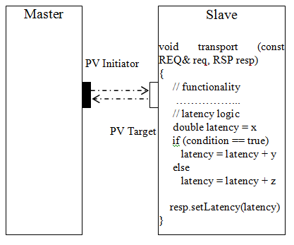
In the above example the communication between master and slave happen using transport API. It is a bidirectional blocking interface and is used to model transactions where there is a tight one to one, non pipelined binding between the request going in and the response coming out. The transport function implements the functionality of the slave device and contains the logic for calculating the lumped latency based on the state and the configurable timing parameters of the device.
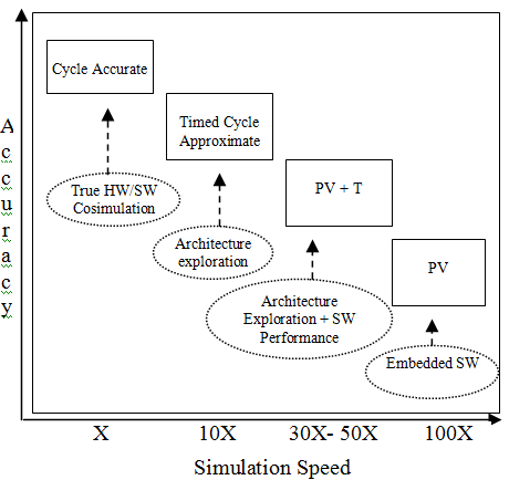
A comparison of accuracy vs simulation speed for a model developed at different abstraction levels are shown below:
L2CC Case Study
We have taken the case study of L2CC for doing the timing annotation. The L2CC model has both the slave interface as well as the master interface.
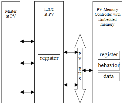
The block diagram shown below reflects the level of information to be present in the L2CC module as required by the pure embedded software developers. The PV L2CC model only needs to correctly implement the all memory mapped register set. We have implemented the register set using the Generic RegFile modeling objects [1]. No functionality related to the cache controller needs to be modeled. This model can be used only for pure software developments. Software analysis or performance modeling can’t be possible using this model. The advantage of this model is that it posses a good simulation speed.
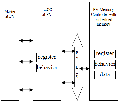
The block diagram shown below reflects the level of information to be present in the L2CC module as required for software analysis. The PV L2CC model needs to correctly implement the all memory mapped register set alongwith the cache controller functionality. Neither timing related logic nor embedded cache memory needs to be present within the module. This model can be used for pure software development as well as for software analysis. The drawback of this model is that, performance modeling can’t be possible using this model. The advantage is that it posses a good simulation speed.
The block diagram shown below reflects the level of information’s to be present in the L2CC module as required by the architects. The PVT L2CC module will implement the register set, complete functionality related to cache controller, icache and dcache data storage alongwith the lumped latency calculator. This model can be used for accurate analysis of bus and memory. It can also be used for performance modeling. The drawback of this model is it would be a bit slower as latency logic is implemented.
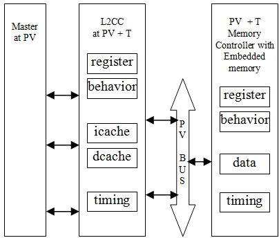
Annotation of L2CC with timing:
Generally software programmable timing parameters present in L2CC register sets are:
-
Tag RAM read latency - This parameter tells the number of clock cycles required by the L2CC to read the Tag RAM. L2CC performs a read access to Tag RAM to find out whether the access is a cache hit or a cache miss.
-
Tag RAM write latency - This parameter tells the number of clock cycles required by the L2CC to update the Tag RAM with the new Tag value.
-
Dirty RAM read latency - This parameter tells the number of clock cycles required by the L2CC to read the Dirty RAM. L2CC performs a read access to Dirty RAM to find out whether the particular cache line is dirty or not.
-
Dirty RAM write latency - This parameter tells the number of clock cycles required by the L2CC to update the Dirty RAM.
-
DATA RAM read latency - This parameter tells the number of clock cycles required by the L2CC to read the DATA RAM i.e. ICACHE or DCACHE.
-
DATA RAM write latency - This parameter tells the number of clock cycles required by the L2CC to write to the DATA RAM i.e. ICACHE or DCACHE.
L2CC calculates the lumped latencies in case of following scenarios:
- Latency in case of read hit
- Latency in case of read miss with the line to be filled is not dirty
- Latency in case of read miss with the line to be filled is dirty
- Latency in case of write hit in write-back mode
- Latency in case of write hit in write through mode
- Latency in case of write miss with write allocate not set
- Latency in case of write miss with write allocate set and cache line to be filled is not dirty
- Latency in case of write miss with write allocate set and cache line to be filled is dirty
Let suppose that the software has programmed the above listed timing parameters to following values:
- Tag RAM read latency - 2 clock cycles
- Tag RAM write latency - 2 clock cycles
- Dirty RAM read latency - 1 clock cycle
- Dirty RAM write latency - 1 clock cycle
- DATA RAM read latency - 8 clock cycles
- DATA RAM write latency - 8 clock cycles
Cache read hit condition:
- Latency for reading Tag RAM
- Latency for reading Data RAM
Total lumped latency for this scenario:
= 10 clock cycles
Cache read miss condition with the line to be filled is not dirty:
- Latency for reading Tag RAM
- Latency for reading Dirty RAM
- Latency for reading the data from the external memory
- Latency for writing the external memory read data into the Data RAM
- Latency for writing/updating the Tag RAM
In this case the L2CC will fetch the complete cache line data from the external memory and put it into the embedded cache memory. Here we are assuming that the memory is returning a read latency of 11 clock cycles.
Total lumped latency for this scenario:
= 24 clock cycles
Cache read miss condition with the line to be filled is dirty:
- Latency for reading Tag RAM
- Latency for reading Dirty RAM
- Latency for reading the Data RAM
- Latency for writing the data to the external memory
- Latency for updating the Dirty RAM
- Latency for reading the data from the external memory
- Latency for writing the external memory read data into the Data RAM
- Latency for writing/updating the Tag RAM
In this case since the cache line to be filled is dirty, the L2CC will first empty the cache line data to the external memory by performing a burst transaction. After that it will fetch a complete cache line data by performing a burst read transaction and put it into the local embedded cache. Here we are assuming that the memory is returning a write latency of 8 clock cycles in case of external memory write operations and a read latency of 11 clock cycles in case of external memory read operations.
Total lumped latency for this scenario:
= 41 clock cycles
Cache write hit condition with write-back mode:
- Latency for reading Tag RAM
- Latency for writing the data into the Data RAM
- Latency for updating the Dirty RAM
Total lumped latency for this scenario:
= 11 clock cycles
Cache write hit condition with write-through mode:
- Latency for reading Tag RAM
- Latency for writing the data into the Data RAM
- Latency for reading the data from the Data RAM
- Latency for writing the data to the external memory
- Latency for updating the Dirty RAM
The L2CC will write the cache line data to the external memory by performing a burst transaction. Here we are assuming that the memory is returning a write latency of 8 clock cycles for external memory write operations.
Total lumped latency for this scenario:
= 27 clock cycles
Cache write miss condition with write allocate not set:
- Latency for reading Tag RAM
- Latency for writing the data to the external memory
Since write allocate is not set and it’s a cache miss scenarios, therefore the L2CC will write the single data as requested by the processor to the external memory. Here we are assuming that the memory is returning a write latency of 1 clock cycle for external memory write operation.
Total lumped latency for this scenario:
= 3 clock cycles
Cache write miss condition with write allocate set, and cache line to be filled is not dirty:
- Latency for reading Tag RAM
- Latency for reading the Dirty RAM
- Latency for reading the data from the external memory
- Latency for writing the external memory data to the Data RAM
- Latency for writing/updating the Tag RAM
- Latency for writing the data from the processor into the Data RAM
- Latency for updating the Dirty RAM
In this scenario the L2CC will first fetch a complete cache line data by performing a burst read transaction and put it into the local embedded cache. It will then write the data received from the processor into the Data RAM. Here we are assuming that the memory is returning a read latency of 11 clock cycles.
Total lumped latency for this scenario:
= 33 clock cycles
Cache write miss condition with write allocate set, and cache line to be filled is dirty:
- Latency for reading Tag RAM
- Latency for reading the Dirty RAM
- Latency for reading the data from the Data RAM
- Latency for writing the data to the external memory
- Latency for updating the Dirty RAM
- Latency for reading the data from the external memory
- Latency for writing the external memory data to the Data RAM
- Latency for updating the Tag RAM
- Latency for writing the processor data to the Data RAM
- Latency for updating the Dirty RAM
In this scenario the L2CC will first fetch a complete cache line data by performing a burst read transaction and put it into the local embedded cache. It will then write the data received from the processor into the Data RAM. Here we are assuming that the memory is returning a read latency of 11 clock cycles.
Total lumped latency for this scenario:
Conclusion:
The basic idea of using the timing annotation concepts is to make the reuse of PV models and with a minimum amount of rework one can come up with a cycle approximate model without compromising much on the simulation speed as well as with a good amount of accuracy.
References:
[1] “Use and re-use considerations when creating SystemC TLM models”, by Sameer Arora, HCL Technologies, www.nascug.org
[2] “Using Programmer’s View Timing Annotation for the creation of Reusable TLM Models”, by Charu Khosla, CoWare, Inc., www.nascug.org
[3] “Transaction-Level Modeling with SystemC”, Frank Ghenassia, Springer, 2005
[4] “Developing Transaction-level Models in SystemC”, by Bart Vanthournout, Serge Goossens, Tim Kogel, CoWare, Inc., www.coware.com
[5] “ARM L210 Cache Controller Technical Reference Manual” from www.arm.com
[6] “System Modelling Transaction Level Modelling”, by Prof. Dr. - Ing. Sorin Alexander Huss
Related Semiconductor IP
- 8MHz / 40MHz Pierce Oscillator - X-FAB XT018-0.18µm
- UCIe RX Interface
- Very Low Latency BCH Codec
- 5G-NTN Modem IP for Satellite User Terminals
- 400G UDP/IP Hardware Protocol Stack
Related Articles
- Leveraging system models for RTL functional verification
- Modelling Embedded Systems at Functional Untimed Application Level
- Refactoring Hardware Algorithms to Functional Timed SystemC Models
- Soc Design -> IP models support codesign efforts
Latest Articles
- SNAP-V: A RISC-V SoC with Configurable Neuromorphic Acceleration for Small-Scale Spiking Neural Networks
- An FPGA Implementation of Displacement Vector Search for Intra Pattern Copy in JPEG XS
- A Persistent-State Dataflow Accelerator for Memory-Bound Linear Attention Decode on FPGA
- VMXDOTP: A RISC-V Vector ISA Extension for Efficient Microscaling (MX) Format Acceleration
- PDF: PUF-based DNN Fingerprinting for Knowledge Distillation Traceability