System Packet Interface (SPI) 4.2 IP Core
Ahmedabad, India
Abstract:
System Packet Interface-4 Phase 2 (SPI-4.2) is a protocol used for data transfer between link layer and physical layer. It is an interface for packet and cell transfer between a physical (PHY) layer device and a link layer device, for aggregate bandwidths of OC-192 ATM and Packet over SONET (POS), as well as for 10 Gb/s Ethernet applications. The SPI 4.2 protocol defines a 311 MHz (minimum) dual data rate (DDR) operation for a 16-bit data bus, effectively yielding a 10 Gb/s data rate. In order to achieve optimum performance, the architecture outlined below does not add any padding data/control packets between two consecutive back-to-back transfers. Also, in order to transfer data efficiently, the architecture incorporates an SPI Performance monitor which reflects the arbitration status and FIFO status measured over a period of time, which can be analyzed by the firmware. This feature helps the firmware to change the calendar sequence or arbitration logic of a specific port, thus achieving a significant improvement in SPI 4.2 channel utilization. Most of the blocks used in the IP are configurable and can also be re-used in protocol implementation of a similar kind.

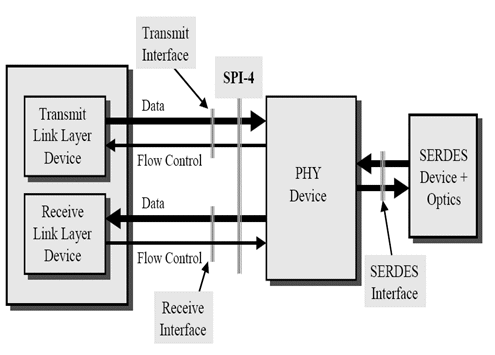
Fig1: SPI 4.2 Link-Phy Layer Interface
INTRODUCTION
The basic top level block diagram of SPI 4.2 interface is as shown in Figure 1. The SPI 4.2 forms an interface between the link layer and PHY device. The SPI 4.2 protocol interface consists of Data and Flow Control signals. It is a source synchronous interface and works at a data rate of minimum of 622 Mbps per line.
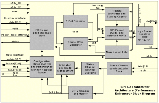
SPI 4.2 is a packet based high-speed protocol. Its basic function is to intelligently multiplex the data coming from link layer, to the SPI 4.2 bus. The receiver is an intelligent de-multiplexer that de-multiplexes the data coming from the SPI 4.2 bus into the respective port’s FIFO. The IP core supports 32 ports each on transmit and receive side. The block diagram of the Transmitter architecture is given in Figure 2.
The input to the transmitter is 64-bit data at 155.50 MHz rate. The output on SPI 4.2 bus is 311 MHz DDR 16-bit data. Hence the input data rates are matching with the output data rates for the transmitter design / architecture.
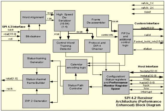
The receiver phase-aligns (static and dynamic alignment) the data received on the SPI 4.2 data bus before sending it to the word alignment and de-serializer block. The receiver de-serializer converts it into 64-bit data and the control word and data control logic separates the data and control words and sends it to the respective FIFO corresponding to the address of the received data. The receiver interface works at 155.50 MHz 64-bit and thus the throughput is 622 mbps.
The detailed block diagram of the receiver section is given in Figure 3.

Fig. 2: SPI 4.2 Transmitter Architecture Block diagram

Fig. 3: SPI 4.2 Receiver Architecture Block diagram
PERFORMANCE ENHANCEMENTS IN THE SPI 4.2 ARCHITECTURE
Zero Idle words between two back-to-back data transfers
The 64-bit data in the FIFO needs to be sent to the output every clock cycle, along with the insertion of 16-bit control words on every new transfer or continuation transfer for another port. Normally, Idle control words can be used for padding transfers which are not multiple of 64bits, in order to align the control words on a certain boundary for insertion. In this performance enhanced IP core, special logic has been used in order to transfer more than one control word back-to-back without any IDLE word in the same clock cycle. Data look-ahead and enhanced frame control logic is used to achieve desired performance level.
Analysis: For a typical data transfer, a 12.5% overhead gets added by the SPI 4.2 protocol [1]. This overhead can increase to 25 - 30 % or more, depending on various data transfer conditions and burst sizes etc. The current IP architecture successfully removes the normal conventional design overhead (due to IDLE padding) and limits the overhead to that added due to SPI 4.2 protocol specifications only. This has been done using techniques to fetch data from the FIFO, frame it and calculate DIP-4 (Diagonally Interleaved Parity) for 64-bit data in a single clock cycle.
SPI Performance Monitor
a. FIFO Performance Monitor: This logic indicates the number of times a particular port was not able to send the data though it won the arbitration. This can be due to non-availability of data in the FIFO or due to watermark levels etc. This can help firmware take appropriate decisions and improve performance.
b. Arbitration Performance Monitor: This logic reflects the number of times a particular port has been accessed between a particular reference start point and end point. (It is usually the time between two trainings.) This will provide some statistics to the firmware, which can then determine if changes in priority are required or not, in a way that may smoothen the probability distribution of access to the other ports.
c. Calendar Performance Monitor: This is just a simple reference as to how many times a port was repeated in the calendar sequence. This data, along with the arbitration data, will help to prune the priorities and calendar sequences. This can be a useful case, when other ports are denied access due to continuous requirement of a particular port on the receiver side.
Low Latency Arbitration and Credit Management
The basic latency in a back-to-back transfer is due to status channel path latency of the receiver and transmitter. The arbitration process takes time due to the pipeline delay of the status path. Typically, this process of waiting for the entire calendar update period can add ~30 % overhead in a SPI 4.2 data transfer (calculated for an Ethernet packet of 1518 bytes and port size (and cal_l parameter) of 256. But due to an improved scheduling mechanism, the IP does not have to wait till the entire calendar is updated. This significantly improves the performance.
It is achieved by assigning credit for the next transfer during the credit assignment for the first transfer. Hence, two credits are assigned during arbitration. Due to this mechanism the next port will immediately start transmitting the data, once the previous data transmission is completed.
Credit management is performed using a fast comparison LUT technique, which also reduces the latency and hence reduces the transfer overhead significantly.

Performance Up-gradation in Interleaved data transfer mode
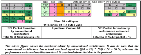
SPI 4.2 protocol suggests interleaved mode, where the transmitter can normally send a packet of only a few data bytes. Usually due to architectural constraints, these kinds of transfers are not considered for proper bandwidth utilization. The performance enhanced architecture mentioned here takes care of these cases and does a packet formation which introduces minimum overhead and thus achieves maximum bandwidth utilization. An example of the same is as mentioned below -
It supports the EC (EOP with continuation) and C (continuation) modes, which are useful for interleaving port data.
Similarly, SPI 4.2 receiver IP core is capable of detecting these control words and interface with the 64-bit data bus.

Introducing Continuation Packets for longer burst transfers
Continuation packets are introduced normally in interleaved transfers in order to send data for a different port without providing the EOP. The architecture mentioned here uses the same for
adding a continuation packet in case of lengthy bursts. There is a burst counter which decrements every clock when data is sent and a continuation packet is inserted when this counter reaches zero.
This is done in order to ensure that the DIP-4 of the previous burst (till the loaded burst count) is sent to the receiver. This ensures availability of DIP-4 to the receiver at regular intervals in case of long bursts. This improves the error correction capability at the receiver. As the DIP-4 is sent at regular intervals, it ensures the DIP-4 checking for shorter bursts rather than a single DIP-4 check for a longer data packet.
The packet formation of the long packet with continuation control word added is shown in figure below. Note that in order to accommodate the entire frame, the example burst count mentioned here is of a lower value.

CONCLUSION
The paper briefly described the architecture of a novel performance-enhanced SPI 4.2 IP Core. It also mentioned, through examples and performance statistics, the improvement in the performance of SPI 4.2 data transfer as against the sub-optimal IP cores available. Normally the protocol adds around 12.5 % overhead for a typical transfer of 16 bytes and other overhead is added by improper architecture. The architecture discussed in this paper, does not add any overhead. Also, this architecture supports data-path over-clocking to eliminate the protocol overheads. The core has been synthesized for ASIC and has shown promising results in gate-level simulation. The architecture provides near-theoretical bandwidth for a continuous data transfer application.
ACKNOWLEDGEMENTS
We would like to take this opportunity to thank Mr. Sudhir Gangaram of Pelican Networks Inc., CA, USA and Mr. Anand S Moghe, Manager, ASIC Group, eInfochips Ltd., Ahmedabad, for providing us invaluable guidance throughout the development of this IP core.
REFERENCES
[1] Optical Internetworking Forum (OIF) SPI Level 4 Phase 2 Specifications – OIF-SPI-4-02.1
Related Semiconductor IP
- NPU IP Core for Mobile
- NPU IP Core for Edge
- Specialized Video Processing NPU IP
- HYPERBUS™ Memory Controller
- AV1 Video Encoder IP
Related White Papers
- Serial Peripheral Interface. SPI, these three letters denote everything you asked for
- A cost-effective and highly productive Framework for IP Integration in SoC using pre-defined language sensitive Editors (LSE) templates and effectively using System Verilog Interfaces
- Rotten to the Core — Part 2: Soft and Vanilla or Hard and Cryptic?
- Achieving multicore performance in a single core SoC design using a multi-threaded virtual multiprocessor: Part 2
Latest White Papers
- Ramping Up Open-Source RISC-V Cores: Assessing the Energy Efficiency of Superscalar, Out-of-Order Execution
- Transition Fixes in 3nm Multi-Voltage SoC Design
- CXL Topology-Aware and Expander-Driven Prefetching: Unlocking SSD Performance
- Breaking the Memory Bandwidth Boundary. GDDR7 IP Design Challenges & Solutions
- Automating NoC Design to Tackle Rising SoC Complexity