Maximizing Performance & Reliability for Flash Applications with Synopsys xSPI Solution
By Lakshmi Jain, Product Marketing Manager and Wei-Yu Ma, Technical Marketing Manager for IO Libraries, Synopsys
Increasing Demand for Non-Volatile Flash Memory
There is a rapidly growing demand for non-volatile Flash memories in the Automotive, AI, and IoT markets for applications that require a fast reading of the massive code base and timely response on the system power-up. Embedded systems utilize non-volatile memory to store boot code, application code/data, AI weights, calibration parameters, diagnostic data, configuration parameters, and other data that persist when the system is powered down. Today, Flash memories fulfil this role in most embedded systems. However, advancements in Flash technology cannot keep up with advances in standard logic technology; therefore, standard logic technology and Flash cannot be mixed on the same die in the most advanced processes.
Systems using SoCs designed in advanced processes generally rely on external Flash devices that use NOR/NAND Flash memory technology for non-volatile storage. NOR Flash memory offers many benefits for device manufacturers and consumers, such as faster reading, low power consumption, and smaller area. In contrast, NAND Flash memories are ideal for applications such as data storage, where higher memory capacity and faster write and erase operations are required.
In this article, we will discuss:
- Critical factors in selecting Flash devices and the specific use cases of NOR Flash memories
- The newly formed first JEDEC standard for Serial Peripheral Interface (SPI) protocol, called eXpanded SPI (xSPI), and how it addresses the rising demands of Automotive and IoT applications
- How Synopsys’ high-performance, high-reliable xSPI PHY and SSI Controller IP solution helps SoC designers accelerate time-to-market and ease design integration

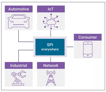
Figure 1: xSPI is everywhere
High Performance and Reliable NOR Flash Memories
For a Flash device used for booting, the performance factor relates not only to how fast the data can be read out of the device but also to how fast the device can be initialized by the system powering on. Automotive applications require a very fast boot time, and IoT applications prefer execution directly on the Flash device.
Amongst the Flash devices available in the industry, the NOR Flash device is typically used to store the bootloader, as the processor can directly run this off the Flash device in what is known as eXecute In Place (XIP).
Several critical factors affect the SoC designer's selection of Flash devices, including device initialization time, XIP capability, and data reliability. If the system needs to execute code directly from Flash (i.e., instead of shadowing to RAM), NOR Flash is the ideal choice. The XIP capabilities in NOR Flash allow the system to reduce the utilization of expensive RAM. Instead of shadowing code to RAM, the processor can execute directly from a NOR Flash device. This approach can reduce the number of pins the processor needs to support the DRAM device, thus reducing PCB and overall system cost significantly. NOR Flash memory typically has a longer endurance than NAND Flash memory because it uses individual memory cells to store data. It is reliable because it utilizes individual memory cells to store data, which decreases the risk of errors affecting multiple pages. Hence, NOR Flash memories are best suited for boot code storage, firmware, and other low-density memory applications because of their reliability, endurance, high performance, and random-access capabilities.
xSPI Interface for NOR Flash Applications
SPI is a de-facto interface across semiconductor applications and nodes for multiple uses (Flash memory, PSRAM, Sensors, TPM interfacing, etc.). The existing SPI interface is limited to the number of IOs and the clock frequency, which has become a bottleneck for system performance improvements.
SPI has been around without standardization for over four decades, but JEDEC has recently announced the JESD251C standard that specifies the eXpanded Serial Peripheral Interface (xSPI) for non-volatile memory devices. Along with the protocol standardization, xSPI provides improved data rate, low pin count and limited backward compatibility with legacy SPI devices. xSPI can work with a single controller and multiple target buses with source synchronous clocking. Since its standardization, xSPI adoption has increased in the Automotive, Networking, and Datacenter markets, especially for devices with expanded boot code sizes.
A versatile set of IO voltage options of 1.2V, 1.8V and 3.3V enables a wide range of support from mature to advanced process nodes. Regarding data throughput, with 400MB/s per pin on an 8-bit IO, xSPI can achieve 400MB/s, a 200% performance improvement compared to Quad-SPI (Table 1). With the XIP ability in NOR Flash applications, the instant-on display data can be processed without loading the boot code into SRAM, a critical requirement for cars with massive displays.

Table 1: Comparison of the SPI growth
Modern NOR Flash devices offer fast initialization time and high bandwidth to minimize boot-up time. The bandwidth can reach 400 MB/s when used with the JEDEC xSPI interface in the Octal or HyperBus bus protocol. Looking at a specific example, a typical U-boot sized between 1 MB to 2 MB with a read bandwidth of 400 MB/s would translate to 5 ms read time, plus a maximum 300 µs device initialization time for the NOR Flash. Compare this to eMMC initialization, which would be ~100 ms and UFS ~50 ms. In addition, if the processor runs XIP directly on NOR Flash, the number of pins is significantly reduced. This results in savings of two to four layers of PCB design, decreasing the overall system cost. Therefore, xSPI is the obvious choice for low-density NAND or NOR Flash memories, as well as PSRAM, which is preferred as a low-cost replacement for internal cache memories against expensive SRAMs.
Achieve Faster Development Cycle with Synopsys xSPI Solution
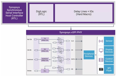
For designers planning to embed Flash memories in their SoCs, Synopsys provides a comprehensive xSPI platform solution (Figure 2) that enables them to reduce the SoC development cycle. The solution includes:
- Synopsys xSPI PHY is a fully integrated hardened macro with high-speed IOs and a delay-locked loop (DLL). The PHY provides impedance matching to ensure signal integrity and higher performance with eight I/Os, eases integration challenges, and provides area-optimized solutions and compatibility with various standards
- Synopsys SSI Controller supports JEDEC xSPI (JESD251B) v1.0 standard, allowing the single IP instance to interact with multiple connected devices, supporting different protocols. Advanced features such as Execute in Place (XIP), subordinate bridge mode, and Internal DMA allow easy access to the serial device and improve overall design performance
The Synopsys fully verified xSPI hardened PHY and Controller offering is complemented by an integration guideline. Additionally, Synopsys performs comprehensive interoperability verification to reduce designers’ SoC implementation effort. This enables seamless integration with devices and peripherals that support these standards.

Figure 2: Synopsys xSPI Platform Solution
Conclusion
With increased adoption of xSPI protocol in Automotive, AI and IoT applications, the comprehensive Synopsys xSPI solution enables SoC designers to seamlessly integrate the latest embedded and removable memory functionalities into their application processors. The Synopsys solution includes a hardened xSPI PHY and an SSI Controller IP, which has been fully verified for interoperability, maximizes the SoC performance and reliability, and reduces time-to-market and cost for Flash devices across FinFET technologies.
For more information, visit Synopsys Specialty IO and PHY.
Related Semiconductor IP
- NPU IP Core for Mobile
- MSP7-32 MACsec IP core for FPGA or ASIC
- 100G / 200G / 400G / 800G / 1.6T MACsec
- 32 bit RISC-V Multicore Processor with 256-bit VLEN and AMM
- UHF RFID tag IP with 3.6kBit EEPROM and -18dBm sensitivity
Related White Papers
- Growing audio requirements in SoCs
- Viewpoint -- USB 3.0: Not just for wired apps
- Leverage video for auto electronics design
- Android hardware-software design using virtual prototypes - Part 2: Building a sensor subsystem
Latest White Papers
- Concealable physical unclonable functions using vertical NAND flash memory
- Ramping Up Open-Source RISC-V Cores: Assessing the Energy Efficiency of Superscalar, Out-of-Order Execution
- Transition Fixes in 3nm Multi-Voltage SoC Design
- CXL Topology-Aware and Expander-Driven Prefetching: Unlocking SSD Performance
- Breaking the Memory Bandwidth Boundary. GDDR7 IP Design Challenges & Solutions