Improving design turn around time on a complex SoC by leveraging a reusable low power specification
NXP Semiconductors
Abstract :
This paper presents an approach to power design specification intent and associated enabled design methodologies that allow a scalable implementation of voltage islands. From a single holistic power specification, power modes are simulated, level shifters, retention logic and on-chip switches are logically inserted, verified, physically implemented and analyzed. Additionally, the power specification should allow hierarchical design flow and IP reuse for designs with complex power architectures. These techniques have successfully been applied on a complex SoC. It was demonstrated that having a common placeholder for capturing the chip’s power architecture avoids error prone recurrent re-entry of the same power intent for each EDA tool and facilitates a scalable implementation. Combined with new tool functionality thus enabled, and a better IP integration, such methodology leads to significant time to market improvement and an optimization of the overall power management scheme.
I. INTRODUCTION
For 65nm and below, with more and more computing power integrated on portable devices, low power is crucial. With latest process technology nodes, channel length, oxide thickness and voltage threshold are smaller, thus increasing leakage power to the point where it becomes as important as active power.
Control of both leakage and dynamic power consumption is now mandatory. Designers have to look beyond the traditional approach minimizing leakage current through the use of multiple threshold voltages or stopping the switching power by gating the clocks.
Leakage can also be addressed by suppressing current, thus switching the voltage to a section of the logic when it is not functionally needed.
Additionally, to meet both chip performance requirements and power goals, new techniques consist in using voltage islands or voltage domains. The most performance critical block of the design would dynamically get the highest voltage supply, when other less critical parts can be run on lower supply, thus saving dynamic power.
But when previous approaches have been mostly solved within the scope a single step in the design flow with point tools, new ones are much more disruptive to the entire design implementation process.
Past SoC designs have clearly identified limitations associated with the design of Multi Supply Voltages SoCs:
- No placeholder for the power and ground nets and to describe power spec and constraints
- No possibility to verify power modes and power sequences in functional simulation.
- No reusability of IPs with multiple power domains into SoCs.
- Tremendous increase of implementation throughput time due to lack of automation.
- Recurrent specification of the same power intent for each tool in the design flow.
- Increase of STA sign-off cases.
- Vast increase of SDF simulation cases, in case of multiple voltage scaling clusters of logic
Among other goals, this SoC was designed to challenge the current architecture and implementation flow. As shown in Figure 1 (next page) it consists in three voltage scalable logic sections, three on-chip switch able domains, six off-chip switch able domains and separate switch able pad ring sections.
The rest of the paper highlights the challenges and solutions used for the design intent description, the verification of power modes and transitions between power states, the scalability of implementation techniques, and discusses some considerations of hierarchical use model. More details on the architecture are presented in [1].
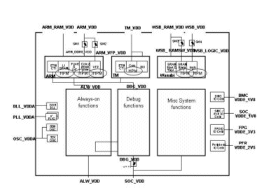
Figure 1: Power domains overview
II. POWER CONNECTIVITY BECOMES PART OF THE FUNCTIONAL DESCRIPTION
In a SoC, Power and Ground nets have traditionally been defined and implemented outside of the scope of the logical design description. Logical views for basic library elements, as well as HDL descriptions did not have implicit representation of these nets as they would not have any functional impact. As a result, they were usually handled at a late stage during physical implementation and usually needed special handling and global connection in the back-end phase. The integrity of their implementation was usually performed by re defining the global nets at LVS stage.
With power islands being turned on and off to minimize leakage current, power nets have now become partly functional as the behavior of the SoC now depends on the state of these signals. The number of voltage islands in SoC and IP designs has increased the complexity of the description of the power architecture considerably. Power and ground nets now need to be specified as part of a design’s functional description and requires a standardized placeholder. From past experiences, the new standard needed to satisfy the following requirements:
- Model power intent (power and ground network) above physical level abstraction of a design.
- Enable functional verification and validation early in the design flow.
- Enable logical and physical implementation of the design from the same power intent that has been verified and validated earlier.
- Enable the verification between power intent modeled at early design stage and the actual implementation of the power intent at the gate level.
- Ease IP reuse and portability
At the time of our SoC design, the standard Common Power Format (CPF) standard published by Si2 (see [3])is the industry first power format to have tool support. The power intent was captured into a CPF while the functionality remained a RTL description, the two constituting our Design Specification (Figure 2)

Figure 2: Design specification components
Such separation, allows the same power intent to be used in mixed languages designs and we can have a simple migration of non-power aware RTL design to power aware RTL design .
A short extract of our SoC’s top level CPF illustrates the power domain partition of our design.
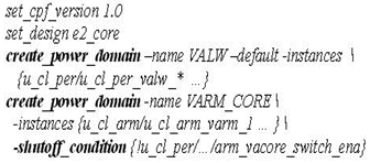
Figure 3: Power domains specification
Two power domains are created at top level. Power domain VALW is the default power domain and it is always on.
The VARM_CORE power domain is a switch able power domain with an associated shut-off condition. An expression specifies the condition under which the power domain will be switched off.
RTL designers do not have to understand the details of how the power domain will be implemented eventually. They can use CPF to describe the power on and off behavior. Through the semantics of power domain, the power behavior for each instance can then be derived such that all instances belonging to the same power domain share the same power characteristics such as voltage, on and off etc. Essentially, the power and ground network and its connections to the instance power and ground pins are modeled through power domain semantics.
Using a complete description of the power network, simple power aware verification was performed by simulating the power up and down behavior of the design.
Later in the flow, designers can associate a power and ground net for each power domain to drive physical implementation. At this later stage only, power nets are actually created as well as associated to the proper power domains.
create_power_nets -nets ALW_VDD
update_power_domain -name VALW_domain -internal_power_net ALW_VDD
This allowed us to separate the power intent from the implementation, the “what” from the “how”, thus exposing the verification community only to the relevant needed information for the verification of power mode and states transitions.
III. METHOD FOR SIMULATING POWER MODES
With 11 power islands, our SoC is representative of an increasing number of designs implemented with multiple voltage islands which can be temporarily powered down to reduce leakage power without affecting the functionality of the rest of the design.
Power shutoff adds another level of complexity to the design verification and must be addressed at the beginning of the design cycle. The fundamental aspects and key questions to be addressed during verification are:
- Isolation: Has logic been added which prevents the propagation of unknown signals to the rest of the design when a block has been powered down? Are the values forced on the inputs driven by power down logic the right values for this block to operate properly?
- State Retention / Initialization: Are the values of key registers stored prior to power being shutoff? How is a block initialized to a known state after power is restored?
- Power Shutoff: Should an entire block be shutoff or portions of the block?
We had in the past managed to verify power down modes either using internally developed PLI/API based routines or by simulating with specially built standard cell libraries where power state functional dependency was crudely modeled. Such methods were not easily scalable and were requiring recurrent specification of the power intent.
The verification environment of our design is software dominated. The test cases are implemented as self-checking software running on either of the embedded CPU cores. A power test case cycles through the various power modes driving the central power mode controller which in turn controls the power-up and -down sequences of the various power domains. For this SoC, we used Incisive Unified Simulator (IUS) to read -in CPF and simulate without changing the RTL. The power shutoff conditions are monitored by the simulator which then powers down and corrupts a power domain when triggered. The power on/off awareness of the simulator is provided orthogonal to the normal simulator functionality, much like assertions. This has proven useful in a number of situations. (Figure 4)
Identifying missing LS and clamps
On our SoC, the implementation choice is made to insert the isolation cells in RTL as opposed to use the existing tool support. However the insertion of isolation cells in RTL isn’t possible for all paths. Typically the infrastructure for production test is generated during, or following the logic synthesis process. Any paths traversing power domains which are created for production test aren’t present in the RTL of the design. Therefore any isolation cells in these paths must be inserted during, or after DfT insertion. The design team opted to insert these isolation cells during the physical implementation phase, by means of using the CPF design description. Then verify the functional integrity by mean of simulation.
Clamping to the proper value
Clamping signals driven from a “power-down” block is necessary but care must also be taken that floating inputs of the “on” block are pulled to the proper logical values for this “on” block to operate properly.
Defining the proper isolation cell value requires detailed knowledge of the inactive state for each IP’s input driven by a power down section. When known these values, in the past stored in spreadsheets or other placeholders can now be captured into the CPF. To facilitate this process in future further standardization is required, which would enable an IP provider to communicate the correct isolation cell value for each pin on an IP through e.g. CPF or IP-XACT.
In absence of such information, especially for legacy IPs, identifying these values proved to be a considerable task, as no comprehensive solution is available. Relying on signal naming convention to derive these values is not a safe approach as signal names are not necessarily consistent and can be ambiguous. (Eg - two active-low reset signals named: ‘N_RST’ and ‘reset_n’). An iterative process was used to verify the voltage domain’s interface in the context of the functional simulation using CPF, and derive the proper clamping.
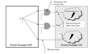
Figure 4: Interface verification for power switching
Identifying incorrect functional behavior in communication spanning power islands
The control network in our design enables communication between IP cells in a number of power domains. To achieve this, the control network implements a number of power domain crossings. A potential risk of this architecture is that communication maybe attempted to an IP cell that is in power down. Due to the power down the IP cell is unable to respond, which in turn might cause a deadlock on the control network. To overcome this potential deadlock the control network implements a timeout mechanism which will abort an ongoing transaction if one of the parties doesn’t respond. During CPF-enabled simulations was proved very useful to the design team to detect that the implementation of this timeout mechanism had been incorrectly placed in a domain that powered down itself, thereby disabling the timeout function itself.
Power aware modeling beyond RTL
Today’s implementation of corruption of powered down domains within IUS works well with all the HDL constructs within this SoC, both Verilog and VHDL. From our experience, the enhanced capabilities of IUS in combination with the CPF description of the design allowed the design team to verify a range of power modes. These test cases uncovered a number of issues that would have been less easy to detect in previous designs.
Going forward, we found that requirement for higher level modeling quickly was needed. Within a simulation environment typically a number of IP cells are replaced by behavioral models for a range of reasons (including simulation performance and availability of RTL code). The verification team found that most of these models don’t respond well to the corruption of a power domain in which they are instantiated. Further effort on power aware behavioral models should be pursued.
IV. HIERARCHICAL USE MODEL
With the design specification now consisting of a {Power Intent, Functional Specification} pair, it is important to be able to define a hierarchical precedence mechanism in order to reuse existing IP specification or constrain an IP implementation. Several obvious use cases illustrated in Figure 5 have to be accounted for:
- Bottom-up reuse: Power design intent has been developed together with an IP. For a soft IP, it should be reusable for the integration of this IP without having to rewrite the intent specification of the entire SoC. In the case of a Hard IP, the power intent should be derived from the IP implementation and such description should also be usable to give IP visibility from the chip level for integration.
- Top-down constraint of lower level IP implementation: Chip level power design intent is created. Low level blocks should have their power design intent derived from this chip level description.
- IP implementation with visibility of the context of its instantiation: IP implementation is done with the knowledge of the power domains at its boundaries. Some of the requirements are illustrated in the next section.
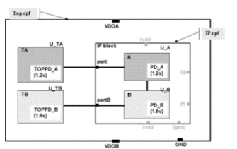
Figure 5: Hierarchical use model
Although slightly more complex, the requirements for proper hierarchical support have similarity with timing constraints, timing models and timing budgeting.
V. SCALABLE IMPLEMENTATION
Experience has shown that EDA tools had so far mostly build patches to enable low power design with new design components. Such ad hoc pragmatic approach however lacks fundamental holistic view and usually affect throughput time of the implementation. We had in some cases experienced 2X productivity drop for the back-end implementation phase. In addition to lack of tool functionality in various areas, this productivity penalty was due to the lack of scalability of the proposed approach to implement voltage islands.
- Addition of interface logic, whether it is isolation gates for power switching or level shifters for voltage scaling, does introduce additional verification challenges. Checks need to be run to verify proper isolation, proper connectivity to the right power domains, proper partitioning of the netlist, proper behavior of the interface and more.
- Similarly, a key characteristic of the level shifter is that it is a standard cell operating with two voltage supplies, thus creating a constraint for the layout implementation.
- Always-on logic resulting from buffering of control logic for retention or global nets in power down blocks requires special care for proper connection of their supplies.
- Voltage islands and on-chip switches create a challenge for power distribution and limit the floorplan alternatives and flexibility. More effort is necessary for connecting power sources to the voltage domains.
- Communication between voltage islands may create logical path spanning power domains boundaries. This creates challenges for sign-off by increasing the number of corners and modes hence the number of STA runs.
It has not been sufficient for tool vendors to address these areas by simply providing the basic low level hooks in their tool infrastructure. Tools understanding the same power design intent with the highest possible level of abstraction are needed to compensate the throughput time overhead introduced by designing with multiples supplies. Following are examples of improvements introduced by CPF.
Power logic Insertion
The rules governing interfaces between different power domains could be easily described in CPF by adding isolation rules and/or level_shifter rules only once. The specification (see Figure 6) allows the highest possible abstract level with a concept of from/to describing signal interaction between power domains.
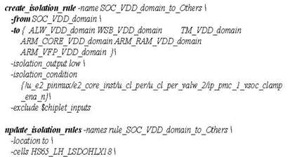
Figure 6: Isolation rules specification
Not having isolation logic inserted in your RTL and having it specified with respect to power domain makes the specification agnostic to changes to the power domain or the RTL, thus allowing a generic and scalable methodology.
For the project, besides being used by simulation tool Incisive Unified Simulator (IUS), the rules defined in CPF allow Logic synthesis tool RTL-Compiler to inserts the power logic, i.e. isolation and level shifting cells, after the DFT synthesis. The same rules also allow Physical synthesis tool SoCEncounter to place these special cells concurrently with the standard cell placement. In addition, power check tool like Conformal Low Power checks the implementation of the special low power logic against CPF isolation rule intent.
Secondary power pin connection
In this SoC, the Wasabe, key infrastructure IP, is the heart of the memory access network. It operates at one supply voltage WSB_VDD_D only, but interfaces with a number of other voltage domains as shown on Figure 1.With the interface logic such as level shifters on the receiving side of the signals spanning voltage domains, special attention needs to be given to the these cells for
- Proper connection and routing of the secondary supply voltage vddin
- Uncontrolled buffering of input signals to the level shifters.
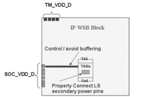
Figure 7: Power domains interface on Wasabi
Methods where the chip level power domains, TM_VDD_D and SOC_VDD_D are made visible during the bottom-up block implementation greatly improves the automation and remove special handling of these cells. CPF provides the notion of virtual power domains ( Figure 8) to which pins of the IP block are associated, thus providing the information about their power domains in the instantiation.
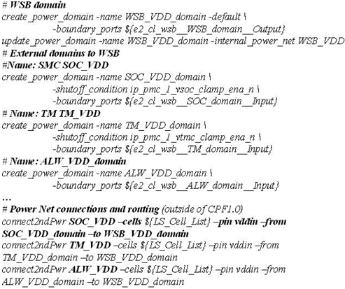
Figure 8: Virtual power domains
This allows a seamless implementation of the level shifters regardless of the number of domains.
Handling modes and corners complexity
The system power reduction of our SoC is achieved by combining component level modes for which the voltage can be static or vary. This greatly increases the number of system level modes making it important to be able to capture these modes and how the transitions between them are governed.
The following modes were created in which each power domain specifies a nominal voltage condition.(see Figure 9 )
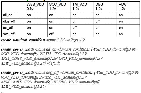
Figure 9: Power modes
With DVFS, an “active” block may mean a range of operating voltages and therefore a large number of corners. Unless attention is dedicated to them, signals between voltage islands can be challenging. For instance, on a synchronous path, besides the presence of interface logic, the hold condition should theoretically be signed –off with the highest voltage on the driving domain and the lowest voltage on the receiving domain. However, it is likely that intermediate operating points will need to be verified as well.
In this design, we reduced the potential timing issues on path spanning across power domains by making them asynchronous (See [3] for more details). Still, performing timing optimization and sign-off verification can be a daunting task due to the number of corners to verify, and a never converging iterative process.
As described in Figure 10 being able to associate analysis views to each power mode, thus raising the level of abstraction gave us the ability to manage the different constraints and library associated to each operating condition of each power domain for each mode.
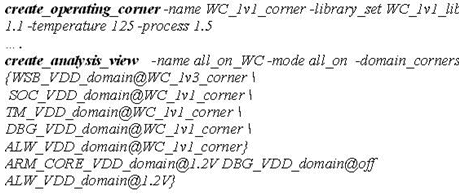
Figure 10: Analysis views
With this centralized approach to the specification in a single place holder and the tool support, the power modes and operating conditions are concurrently taken into account during synthesis, optimization, STA, and formal verification in a multimode multi-corner analysis and optimization flow.
This section has shown through a few example how the overhead associated with the complexity of designing with multiple supplies is greatly removed by the scalability of the solution.
VI. CONCLUSION
In this paper, we walked through a multi supply voltage implementation of an SoC in which power design intent has been specified using CPF, a standard placeholder , non intrusive and incremental, published by the Si2 Low Power Coalition.
Managing the power and ground networks through a golden reference, performing a power aware functional simulation, having a proper tool support and methodology during implementation for insertion, placement and special routing of interface logic, multi-mode multi-corners optimization, have alleviated many of the expensive manual tasks required in the past on such designs. The overhead associated with the complexity of designing with multiple supplies is greatly reduced by the scalability of the solution.
In addition, although not necessary for this first experience of using a standard, the hierarchical paradigm for a reuse of such specification and subsequently the requirements for an IP delivery have been highlighted.
Although not used to its full extent, CPF1.0 has proven a solid foundation to build upon. Further improvements and higher level extensions have been identified. They should be discussed and proposed in the industry level Low Power forums NXP contributes to.
ACKNOWLEDGMENTS
The authors gratefully acknowledge the entire design team for their dedication and successful completion of the project.
The authors also acknowledge Si2 LPC for their effort towards standardization of the low power intent and the fruitful discussions with industry representatives to articulate future requirements in this field.
REFERENCES
[1] N. Wingen “What if you could design tomorrow's system today?” Design, Automation, and Test in Europe, pp. 835 – 840.
[2] A P Niranjan and P Wiscombe "Island of Synchronisity, a design methodology for SoC Design “ Design Automation and Test in Europe, Feb.2004 pp.488-491.
[3] Silicon Integration Initiative – Low Power coalition – Si2.org
Related Semiconductor IP
- NPU IP Core for Mobile
- MSP7-32 MACsec IP core for FPGA or ASIC
- UHF RFID tag IP with 3.6kBit EEPROM and -18dBm sensitivity
- NPU IP Core for Edge
- Specialized Video Processing NPU IP
Related White Papers
- A versatile Control Network of power domains in a low power SoC
- Integrated Low Power Verification Suite: The way forward for SoC use-case Verification
- Low Power Design in SoC Using Arm IP
- Achieving Lower Power, Better Performance, And Optimized Wire Length In Advanced SoC Designs
Latest White Papers
- Ramping Up Open-Source RISC-V Cores: Assessing the Energy Efficiency of Superscalar, Out-of-Order Execution
- Transition Fixes in 3nm Multi-Voltage SoC Design
- CXL Topology-Aware and Expander-Driven Prefetching: Unlocking SSD Performance
- Breaking the Memory Bandwidth Boundary. GDDR7 IP Design Challenges & Solutions
- Automating NoC Design to Tackle Rising SoC Complexity