A Cost-Optimized Set-Top Box Architecture
Abstract:
This paper presents a cost-optimized system on chip architecture for cable-based high definition TV set-top box platforms with integrated DOCSIS channel bonding and high speed home networking.
The architecture has several features which lower its system cost, including high-levels of integration, supporting contiguous memory over multiple independent memory controllers and support for very low power management.
1. Introduction
Current developments in the provision of all-digital interactive TV and domestic internet services have been driven by increased functional demand by the consumer, increased price competition among service providers and international green initiatives.
Customer requirements are directed towards an expanded number of services requiring higher data bandwidths and an ability to easily update software. For service providers, higher bandwidths support additional revenue streams such as video-on-demand, home networking, gaming and web-based services. A key issue for service providers is to drive down the cost of set top boxes (STBs) which can offer these new services. Several standards have arisen whose goal is to increase competition amongst STB manufacturers by removing proprietary technology barriers. It is likely that in the near future that the power consumption levels of STBs will be classified and will become critical in the marketing of these devices.
This paper describes a new architecture which addresses these next-generation requirements and discusses the emergent architectural trends in this class of consumer device.
2. Context
In the Cable TV and broadband market the introduction of DOCSIS[10] channel bonding allows a high bandwidth network connection to a subscriber's home, enabling a transition from a traditional video broadcast model to an IP multicast model. This "fat pipe" means an increased number of HD video streams, including on-demand content and interactive services can be delivered in a set-top box with integrated cable modem. The latest plans from the largest North American cable TV operators target products with an expected life span of 7 years. By supporting user downloadable applications through a Java based middleware new features can be added at any time. The required JVM as well as an unknown amount of compute power for the applications leads to a steep increase in CPU requirements. The amount of compute power required for network processing within these devices is driven not only by the channel bonded DOCSIS, but also home networking and an upcoming transition to IPv6 on operator networks. Against this background of ever-growing functionality, the industry faces a push towards lower power implementations. Forthcoming legislation is likely to mandate a standby consumption of less that 1 Watt. Contemporary, less feature-rich, set-top boxes consume approximately 30 Watts in standby [1].
By specifying a common middleware (CableLabs Tru2way) as well as standards-driven security, for example Multi-Stream CableCARD and DLNA/DTCP, the operator can chose from a large number of vendors for its set-top boxes, leading to increased cost pressure. To further reduce operating costs operators wish to use the box's cable modem to deliver diagnostic information to their head end. This implies that the cable modem must be robust to software malfunctions in the video portion of the platform.
The described architecture aims to increase the level of SoC integration within the set-top box and to optimize the memory system enabling the implementation of powerful, low-cost products.
3. Architecture
This architecture can be considered as the integration of the highest performance HD AVC decoding back-end in the industry with the highest performance cable modem front-end available.
We conducted a systems review of contemporary designs in this space with the goal of identify those aspects which would have the largest effect on lowering overall system cost but could achieve the flexibility necessary to meet anticipated requirements. This architecture is our attempt at producing a design which improves significantly on those which have gone before.
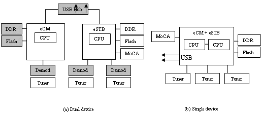
Fig. 1: Architecture Comparison
CPU
In order to service the processing requirements an unprecedented amount of CPU power was added to support the application software model. This allows headroom not only for the downloadable Java applications but also the emerging network processing loads. The deployment of Symmetric Multi-processors are imminent in this space. However, today, a good balance between the requirements of legacy software and performance is to implement a homogenous asymmetric multi-processor (AMP) architecture. We decided to use two super-scalar 32bit RISC host CPUs with vector floating point units. Both CPUs see an identical address map which, combined with a steerable interrupt controller, allows high flexibility in the allocation of processing to CPUs. The use of a full interrupt routing crossbar between the host CPUs and the other CPUs gives a lot of flexibility when allocating processing to CPUs. This is critical not only to support the downloadable application model but also when standard use-cases are confirmed late in the design process and so we need to supply both high performance and high flexibility.
This architecture is implemented by a pair of ST40-300 CPUs [2], and a pair of ST231 VLIW CPUs all four running at 450MHz, delivering a total of 2600 Dhrystone MIPS.
Memory
In order to minimise DRAM cost an analysis of the memory use of an embedded cable modem (eCM) and an embedded set top box (eSTB) was performed. The best cost/performance trade-off was found to be by implementing two 16-bit DDR2-800 interfaces. This arrangement brings the ability to populate system memory with a non-power of 2 megabytes. For example, applications requiring 384MB can be supported directly rather than having to over specify a 512MB system.
A pair of memory interfaces has the advantage of having a higher peak efficiency than a single interface of double the width. It can also simplify the task of bandwidth sharing between very high-bandwidth relatively latency-tolerant IP like video decoders and much lower bandwidth but relatively latency-sensitive IP like CPUs. However, in practice higher performance can only be attained if the bandwidth requirements between the two DRAM controllers is balanced.
The memory architecture is able to abut the memory regions allocated to each DRAM controller. This means that linux implementations do not require discontiguous memory support and the memory wastage which accompanies hardware partitioned memory spaces can be avoided.
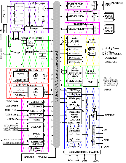
Fig. 2 The topology of the NOC
Architecture analysis revealed that by using a 64KB SRAM buffer to aid DOCSIS packet processing the external memory bandwidth was reduced, and the need for hardware packet filters was avoided. In particular by DMA-ing DOCSIS packet headers directly into on-chip memory allowed a 7-fold decrease in latency enabled us to remove the necessity for the CPU to access packet buffers held in DRAM for packets which would be ultimately discarded.
A key challenge was to support a high-speed secure boot from the lowest-cost flash which gives the capacity and performance required by the customer.
Boot time is an important parameter for set top boxes and contemporary designs are commonly criticized in this aspect. Crucially, by selecting a CPU with 16-bit instructions we were able to significantly diminish the application footprint compared to other CPU architectures with 32-bit ISAs. For example, the flash image size of the linux kernel is 1.4x larger with a MIPS32 4K processor than with an ST40-300. This not only means that Flash size may be reduced but that booting can be quicker.
Integration
Further cost savings are made through the integration of multiple QAM demodulators and the fact that the eCM and eSTB can communicate via shared memory, rather than over a USB interface, see Fig.1 [4].
Network on chip
The problems of bandwidth scalability, high area occupancy and high power consumption meant that we had to look beyond the type of first generation networks on chip implemented in current chips carrying STBUS, AMBA or OCP-IP protocols.
The central interconnect of the chip implements a protocol-neutral switch of high-speed narrow connections. At the boundary of the switch are a set of network interfaces (NI) which are able to convert between a protocol based switching medium (STBUS) and a flit-based network on chip.
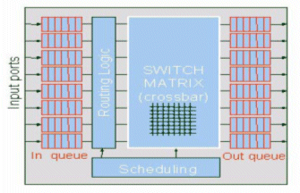
Fig.3 A network on chip
This arrangement meant that timing could be easily met at an interconnect clock rate of 200MHz – which hitherto had always been an issue.
Software architecture
The statically partitioned software architecture is shown in Fig.4, see also [9]. By using OS21 as a lightweight RTOS on one CPU prompt handling of DOCSIS MAC management frames is ensured. Running Linux on the other CPU provides an application-friendly platform for middleware and the customer’s differentiating software. In order to make best use of the total processing capacity, a task previously in the domain of the eSTB, decapsulating video which arrived over a network interface, can be off-loaded to the CPU running the eCM. The decapsulation task then injects the recovered streams into the transport subsystem of the eSTB. To the eSTB application it appears that the video arrived as a standard video broadcast thereby enabling a large amount of software reuse.
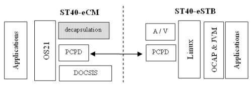 Fig.4: Software architecture
In order to support application robustness across a dual-processor architecture it was necessary to enhance the way that watchdog timers (WDTs) are normally used in the event of software failures. By providing 3 watchdog timers, one CPU can be designated the master, the other the slave. If the slave CPU WDT triggers it resets itself and sends an interrupt to the master, the reset of the system continues to run. On servicing the slave’s reset interrupt the master CPU can execute the diagnostic routines and report to the headend over DOCSIS. If either the system WDT or master WDT trigger the entire device can be reset.
The security infrastructure has the responsibility to restrict which data flows are allowed. Each instance of the device will have its security configured in order to limit IP to being only able to access those areas the software architect decrees is necessary for the correct functioning of the part. It was necessary to extend this infrastructure to prevent the eCM and eSTB subsystems from corrupting each others memory region
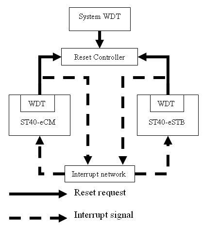
Fig. 5: Watchdog timer deployment
4. Low Power
With current technology there are a myriad of different power saving techniques at the architectural, integration and IP design levels. Due to industry initiatives, legislative mandate, and environmental issues it became key that this chip exhibited the lowest power consumption possible.
The first thing that we did was increase the number of independent clock domains from, typically 3-4, to 18-20 (dependent on configuration) to give finer grain control of IP level clock gating.
We also implemented an agile clocking scheme with support for per-domain dynamic frequency changing and per-domain clock gating; allied with smart, operating-mode aware, low power software drivers, this allows the dynamic power consumption of the device to match the task being performed. Thus we achieve the goal of the device appearing to be on and responsive to the head-end, whilst operating in a low-power state.
Implementing the device in a half-node optical shrink (55LP) of an existing, low leakage, process (65LP) allows an instant power saving of approximately 10% compared to the full node.
The DDR2 DRAM controller specification was enhanced to support transparent auto entry into an Auto-Precharge Power-Down mode (APPD) when the memory is infrequently used. This can save up to 90% of the power consumed by the memory devices in an idle system, with no impact to the software running on the device.
By aggressively integrating system functionality into the device a number of external components, including multiple QAM demodulators, and a USB hub can be removed from the set-top box. The unification of the memory map between the DOCSIS cable modem and the set-top box host processor and IP removes the requirement for dedicated Flash and DDR memories, bringing a reduction in chip count and significant power saving.
Supporting boot from NAND Flash allows the system designer to remove the small NOR boot Flash traditionally found in systems using a high capacity NAND component for mass storage.
The dual memory interface architecture allows the storage associated with video decode and display to be placed into a low power state without affecting the operation of the other processes within the device. A dual CPU architecture allows the macro functions, eCM & eSTB, to enter low-power states independently.
We estimate that this will help STBs to an average 50% power saving over the current generation. In the UK alone this would represent a saving of 3.2TWh/year or 2 million tonnes of CO2 per annum.[1]
5. Conclusion
In this paper we have outlined how we optimized a highly complex SoC for cost, performance and power whilst having the flexibility to deal with evolving specifications and a downloadable software model.
We used a flexible multi-core CPU architecture because it met the requirements of legacy software and provided sufficient performance at low power. By focusing on an optimal memory architecture and super integration a lower bill of materials for this new generation of set-top boxes is possible. Robustness and diagnostic facilities are provided by integrating the CPUs with this in mind and by leveraging the existing security infrastructure. The regular nature of this architecture allows for rapid silicon and software design, a 160 million transistor device was fabricated in a 65/55 nanometer processes. An early floorplan is outlined below (not strictly to scale).
6. Acknowledgements
Thanks to Neil Frost, Michel D’Hoe and Jean-Yves Danckaert for their continued expertise in this technology. As usual we relied on an outstanding SoC design team at STMicroelectronics Bristol, in particular, Paul Ravenhill, Claire Bonnet and Davide Sarta for their experience, insights and pragmatism in implementing these architectural techniques. That this chip has been completed and brought to market on time owes much to our project manager Andrew Lunness.
7. References
[1] NRDC Study of Set Top Box and Game Console Power Use
[2] S. Narita, "SH4 RISC Microprocessor for multimedia, gaming machine" IEEE Design, Automation and Test in Europe, 2001.
[3] R. Deaves and A. Jones, “A Toolkit for Rapid Modeling, Analysis and Verification of SoC Designs”, IPSOC, Nov. 2003.
[4] MoCA Organization, “Cable and Satellite Digital Entertainment Networks”, white paper, 2007.
[5] M. Grimwood et al, "Enhancing the DOCSIS cable modem specifications with an advanced physical layer for upstream transmission", in IEEE ConsumerElectronics, 2000.
[6] R. Deaves and A. Jones, “An IP-based SoC Design Kit for Rapid Time-to-Market”, IPSOC, Dec. 2002.
[7] W. J. Dally, B. Towles - Principles and practices of interconnect networks - Morgan Kaufmann Publishers, ISBN 0-12-200751-4
[8] A Jones & S. Ryan.A re-usable architecture for functional isolation of SoCs. IP 07 – IP Based Electronic System Conference. Dec 2007
[9] R Deavs, A Jones, M Habets & S Ryan Embedded Software Architecture specification developments in support of SoC design and reuse. IP 08 – IP Based Electronic System Conference. Dec 2008
[10] www.cablemodem.com for DOCSIS (Data Over Cable Service Interface Specification)
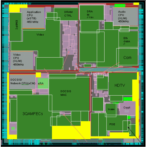
Fig. 6: An early floorplan of the chip
Related Semiconductor IP
- NPU IP Core for Mobile
- NPU IP Core for Edge
- Specialized Video Processing NPU IP
- HYPERBUS™ Memory Controller
- AV1 Video Encoder IP
Related White Papers
- A UML Representation of a Passive Standby Power Management Architecture for Set-Top Boxes
- Consumer IC Advances -> 'Future proofing' set-top box design
- Initial Investigations into UML Based Architectural Reference Patterns for Set-Top Boxes
- Reconfiguring Design -> C-based architecture assembly supports custom design
Latest White Papers
- Ramping Up Open-Source RISC-V Cores: Assessing the Energy Efficiency of Superscalar, Out-of-Order Execution
- Transition Fixes in 3nm Multi-Voltage SoC Design
- CXL Topology-Aware and Expander-Driven Prefetching: Unlocking SSD Performance
- Breaking the Memory Bandwidth Boundary. GDDR7 IP Design Challenges & Solutions
- Automating NoC Design to Tackle Rising SoC Complexity