A RTCA-DO-254 Compliant Development Process for Supporting the Design of High-Quality Hard IP Cores
By Patricia Lira1,2 and Edna Barros1
1 Federal University of Pernambuco, Informatics Center - UFPE
2 Centro de Tecnologias Estratégicas do Nordeste – CETENE
Recife, Brazil
Abstract:
The increasing structural complexity and the decreasing size of integrated circuits, associated with the reduction on design time, demands that the hardware designer uses a very well planned design flow to obtain high quality IP-cores.
With increasing demand on more complex IP-cores, mechanisms for guaranteeing the design quality are being standardized and must be included in the design flow. The DO-254 standard is an example of such standardization for airborne systems.
In this context, the availability of a Development Process for hardware is an effective support for having defined a set of ordered steps for designing high quality digital systems. The ipPROCESS is a process for designing high-quality Soft IP-cores that has supported the design of IP-cores from its specification until its prototyping in FPGA. However, quality standard for digital systems includes also the prototyping as ASIC.
This paper proposes an improvement of the current ipPROCESS version, which includes all flows and activities for designing high-quality hard-IP-cores including synthesis, test and layout generation. For this purpose, three news disciplines have been included in the ipPROCESS; the disciplines for Synthesis, for Test and for Back-End. Each discipline includes the workflow of all activities, Roles and Artifacts. For validating this new ipPROCESS release a LCD controller has been designed from this specification until ASIC prototyping. Using the ipPROCESS for guiding the synthesis, test and layout design has reduced the design time in 50%. Additionally the last version of ipPROCESS is 100% compliant with the requirements of DO-252 standard which makes the use of the ipPROCESS very interesting for supporting the design of IP-cores that must be certified according the DO-254 standard.
1. INTRODUCTION
The complexity of the integrated circuit systems and the enabling integration technologies allow to integrate the whole system into a single chip, called SoC (System-on-Chip). On the other hand, due to the reduced time-to-market, IC design methodologies are using reusable components previously designed, the IP-cores, as an alternative to facilitate the design of a complex and complete system.
Additionally, the increasing structural complexity and the decreasing size of integrated circuits, associated with the reduction on development time, demands that the hardware designer uses a very well planned design flow. Designers have, therefore, increasingly adhered to rigid, rapid and consistent design methodologies that are more amenable to design automation.
In this context, the usage of a Development Process seems to be an effective approach to define the design flow as a set of well defined and ordered steps to guarantee the design high quality integrated circuits.
As mentioned, the current version ipPROCESS supports the design of soft IP-cores with prototyping in FPGA. This work proposes a new version of the ipPROCESS that supports the activities of synthesis, test and layout generation for ASIC prototyping of hard IP-cores.
2. RELATED WORKS
In this section we briefly discuss some related works in the area of process development for software design and the DO-254 standard for designing critical systems in hardware.
The Rational Unified Process [1][2], RUP is a process framework developed by the Rational Software Corporation, from IBM, in 2003. The RUP presents an iterative view of good practices to software development and project management, which is being used in thousands projects worldwide.
RUP is composed for six engineering disciplines modeling, requirements, analysis & design, implementation, test and deployment - organized along four project lifecycle phases – conception, elaboration, construction and transition. A software team that wants to develop a project based on RUP can customize the appropriate process elements that meet their needs.
One of the RUP advantages is to be a process iterative and incremental. The iterative process helps to manage the changes on the project requirements, while the incremental method aids the project team to show previous system version to the client and avoids an implementation that diverge from the real client needs.
Another related approach in the area of software development is the eXtreme Programming (XP) process [3][4]. It was created by Kent Beck, based on his work on the Chrysler Comprehensive Compensation System payroll project[5]. Some development practices purposed by XP are pair programming, test-driven development, continuous integration and a development divided in small releases.
RTCA DO-254[6], Design Assurance Guidance for Airborne Electronic Hardware, is a standard used for design assurance of airborne electronic hardware. The document classifies the design in five design assurance levels A-E, in which the failures in projects with level A represents the bigger security influence.
3. THE ipPROCESS DEVELOPMENT PROCESS
The ipPROCESS[7][8] is a process to develop Soft and Hard IP-cores from its specification until its FPGA and ASIC prototyping. It is currently on the version 3.0 and its main goal is the development of high-quality IP-cores that meets the design constraints. To achieve this, the ipPROCESS provides a disciplined approach to assigning tasks and responsibilities within a development organization and is based on Software Engineering techniques, supported by processes such as RUP (Rational Unified Process) [1] and XP (eXtreme Programming) [2]
Figure 1 presents the key concepts to understand the general structure of this process and how the elements as correlated.
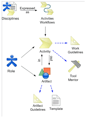
Figure 1. ipPROCESS Key Concepts.
The concept of discipline has been incorporated from RUP, in which the discipline is defined as a collection of activities related with an “area of concern” of the project. It is composed of a set of discipline workflows that describes a sequence of activities with begin and end.
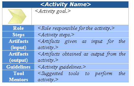
Each activity is a work unit executed for a responsible that represents a role in the project. The activity has a set of ordered steps and a set of inputs and outputs artifacts. An activity can be supported by some work guidelines and suggested tools. The Table 1 shows an example of the activity template.
Table 1. Activity template.
Roles are composed by a set of responsibilities and behavior that a person has to assign to execute some activities in the context of the development organization. It can be represented by a single or a group of person.
Artifacts are a work product of the project that has as responsible the role associated to the activity that generated it.
Figure 2 shows the four ipPROCESS phases: conception, architecture, RTL design and prototyping. Each phase is essentially a span of time between two major milestones. At each phase-end, an assessment is performed to determine whether the objectives of the phase have been met. A satisfactory assessment allows the project to move to the next phase.
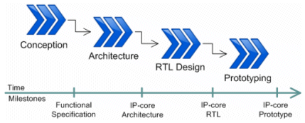
Figure 2. ipProcess phases.
Figure 3 shows the proposed ipPROCESS Lifecycle Diagram. It indicates the disciplines and the effort done in each discipline along the design’s phases and iterations.
The proposed ipPROCESS is composed by 8 disciplines that support the design of an IP-core starting from requirements capture until the prototyping in FPGA or as ASIC.
The disciplines are described in terms of activities (that group related tasks), workflows, artifacts, and roles, occurring in this order:
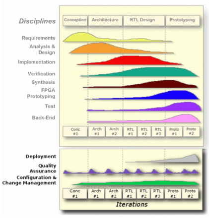
Figure 3. ipPROCESS Lifecycle Diagram.
- Requirements: includes 5 activities, 7 artifacts, 5 templates, for establishing and maintaining agreement with the customers on what the IP-core should do.
- Analysis & Design: includes 3 activities, 8 artifacts, 3 templates for transforming the requirements into a design of the IP-core.
- RTL Implementation: includes 6 activities, 4 artifacts and, 2 templates and 1 script for implementing the components, according to the IP-core architecture in some HDL.
- Functional Verification: includes 8 activities, 7 artifacts, 3 templates and 1 script for evaluating through functional verification and assessing the IP-core quality, finding and documenting defects.
- Synthesis: includes 5 activities, 9 artifacts, 3 templates and two scripts for doing the RTL and logical synthesis for obtaining a net-list according a given technology library.
- Prototyping: includes 8 activities, 5 artifacts, 1 template and 1 script for prototyping the IP-core in the FPGA, based on the implementation components.
- Test:: includes 5 activities, 10 artifacts, 4 templates and scripts for generates a net-list with test structure and test-vectors.
- Back-end: includes 7 activities, 8 artifacts, 1 template and 1 script for generating the layout and encapsulating of the IP-core.
Additionally there are 3 disciplines that support quality assurance and infra-structure support:
- Deployment,
- Quality Assurance
- Configuration & Change Management.
For these disciplines more 28 activities, 29 artifacts, and 19 templates have been defined for supporting the deployment of the IP-core as well activities for guaranteeing the IP-core quality.
This paper focuses on the flow for supporting ASIC design with the development of 3 newer process disciplines: Synthesis, Test and Back-End, which will be detailed described in the next sections.
3.1 SYNTHESIS DISCIPLINE
The Synthesis discipline groups the activities to perform Behavioral Synthesis and Logical Synthesis. These activities are responsibility of the Synthesis Designer and the Synthesis Engineer as shown in the Figure 4.
The Synthesis Designer is responsible for developing the Synthesis Plan. This plan describes all the planning for the synthesis activities like the technology, tools and environment, design constraints, and the order that the components of the system will be synthesized.
To develop this artifact, the Synthesis Designer must considerate design decisions taken in previous parts of the design development, like the non-functional requirements that should be described on the Requirements Specification.
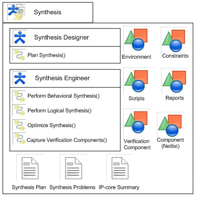
Figure 4. The Synthesis Discipline.
Once the Synthesis Plan has been defined, the Synthesis Engineer can perform the activities to elaborate the synthesis. These activities are grouped in the following disciplines Workflows:
- Perform Behavioral Synthesis – indicates the activities to convert a behavioral description of the IP-core elaborated on the Implementation discipline in a RTL description;
- Perform Logical Synthesis - indicates the activities to converts a RTL description elaborated in a net-list description;
- Optimize Synthesis – responsible for optimizing the activities performed in the previous mentioned disciplines workflows (Perform Behavioral Synthesis and Perform Logical Synthesis) in order to fulfill the IP-core constraints defined in the Synthesis Plan;
- Capture Verification Components – its main goal is to group in the Verification Component artifact all the files and directories that enables the Verification.
3.2 TEST DISCIPLINE
The Test discipline groups the activities to include Design for Testability (DFT) on the IP-core. These activities are responsibility of the Test Designer and the Test Engineer as shown in the Figure 5.
The Test Designer is responsible for developing the Test Plan. This plan describes all the planning for the test activities such as the kinds of test structures to be insert in the circuit, the constraints (that can be more flexible that these ones to the Logical Synthesis) and the minimum test coverage acceptable.
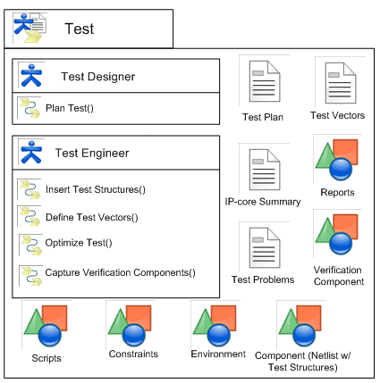
Figure 5. Test Discipline.
Once the Test Plan has been defined, the Test Engineer can perform the activities to perform the Test. These activities are grouped in the following Workflows:
- Insert Test Structures – indicates the activities to converts a netlist description in a netlist with structures to allow DFT;
- Define Test Vectors – indicates the activities to define the test vectors to perform the Test in a manufactured IP-core, inserting the Test Vectors on the IP-core netlist, as well as for analyzing its efficiency and performance;
- Optimize Test - responsible for optimizing the activities performed in the workflow “Insert Test Structures” in order to achieve the design constraints defined on the Test Plan;
- Capture Verification Components - its main goal is to group in the Verification Component artifact all the files and directories that enables the Verification.
3.3 BACK-END DISCIPLINE
The Back-End discipline groups the activities to generate the layout of the IP-core. These activities are responsibility of the Back-End Designer and the Back-End Engineer, as shown in the Figure 6.
The Back-End Designer is responsible for developing the Back-End Plan. This plan describes all the planning for the back-end activities such as the localization and the kind of the IO PADs, the constraints and the kind of verification that must be done during the Validate Activity.
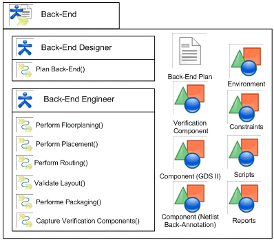
Figure 6. Back-End Discipline.
Once the Back-End Plan has been defined, the Back-End Engineer can perform the activities to elaborate the Back-End. These activities are grouped on the following Workflows:
- Perform Floorplanning – the goal of this workflow is to minimize the chip area and delay problems;
- Perform Placement – it is the workflow activity to place the physical cells, without overlap, with the goal to minimize the connections size;
- Perform Routing – routing is the stage of physical synthesis which is responsible for defining the metal routes and levels;
- Validate Layout – the circuit layout has been synthesized, it is necessary to perform some verification to validate its correctness;
- Perform Packaging – the packaging is responsible to locate the chips in capsules that allow the I/O electrical contacts of integrated circuits to be connected in a conventional circuit board;
- Capture Verification Components - its main goal is to group in the Verification Component artifact all the files and directories that enables the Verification.
4. ipPROCESS COMPLIANCE WITH D0-254
Table 2 shows how the ipPROCESS approach is compliant with DO-254 certification for critical systems. The table includes all artifacts that are required for the DO-254 certification and the artifacts that the ipPROCESS delivers.
Table 2. DO-254 x ipPROCESS.
| DO-254 | ipProcess |
| Hardware Plans | |
| Plan for HW Aspects of Certification (PHAC) | Instance ipPROCESS |
| Hardware Design Plan | Implementation Plan, Verification Plan, Synthesis Plan, Test Plan, Back-End Plan |
| HW Verification Plan | Verification Plan |
| HW Configuration Management Plan | Configuration Management Plan |
| Hardware Process Assurance Plan | Instance for assurance quality |
| Hardware Design Data | |
| Hardware Requirements | Requirements Specification |
| Hardware Design Representation Data | |
| Detailed Design Data | Design Document |
| Top-Level Drawing | Design Model |
| Assembly Drawings | Deployment Model |
| Installation Control Drawings | IP-core Summary, User Manual |
| Validation And Verification Data | |
| Hardware Traceability Data | Traceability Matrix |
| Hardware Configuration Management Records | Hardware Configuration Items |
| Hardware Process Assurance Records | Hardware Configuration Items |
| HW Accomplishment Summary | ipPROCESS instance report |
The PHAC, Hardware Process Plan and Hardware Accomplishment Summary documents are directly related with the DO-254 certification and are under the responsibility of the Quality Assurance ipPROCESS discipline.
This comparison shows that the ipPROCESS can be used for airborne projects that intended obtain the DO-254 certification, covering 100% of the required artifacts.
5. RESULTS
To validate the proposed ipPROCESS release, a LCD Controller has been designed from the requirements until the layout synthesis.
The LCD controller IP-core implements all functionalities of an alphanumeric display LCD. It prints 32 characters in two lines, 16 in each, and possesses several functions to manipulate the printed character. Some of its functionalities are to clear display, to return home, to entry mode set, cursor or display shift, to write characters, display On/Off control. The block diagram for the LCD Controller can be seen in Figure 7.
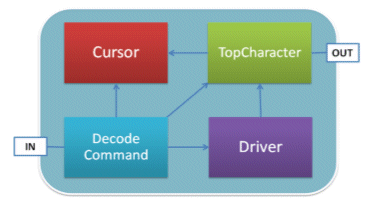
Figure 7. LCD Controller Architecture.
The final layout of the LCD Controller can be seen in Figure 8. Table 3 shows the most important design results.
Table 3. IP-core results.
| Data | Count |
| Logic gate count | ~ 10000 |
| Transistors | ~ 105500 |
| Silicon area | ~ 14 mm² |
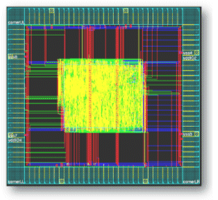
Figure 8. LCD Controller layout.
In the first attempt for design the LCD controller, an older version of the ipPROCESS has been used, that did not include the disciplines for guiding synthesis, test and back-end activities. During this tentative a team of two undergraduate students have worked for four months and they did not have success since the layout had not satisfied the DRC rules.
In the second attempt for design the layout of the LCD controller, the proposed version of the ipPROCESS has been used for guiding the synthesis, test and back-end activities. The design has been successfully done and a team of two undergraduate students have accomplished the design in two months.
When comparing the design using the proposed ipPROCESS version for doing synthesis, test and back-end developed with the proposed methodology has a decrease of 50% of the design time to obtain a final IP-core layout without any violations. Additionally, the IP-core designed using the version of the ipPROCESS is better documented improving the communication among designers.
6. CONCLUSION
In this paper, it was presented the extension of the development process, the ipPROCESS, to include also the flow for Hard-IP cores development. This extension includes 3 new disciplines: Synthesis, Test and Back-End, which have a total of 42 new activities, under the responsibility of 6 new roles and generating 27 new process artifacts.
All commercial and military avionics systems that are prototyped in ASIC or FPGA must be complaint with the DO-254. The ipPROCESS is a process that supports the design of IP-cores (ASIC and FPGA) according to the DO-254 standard, with an optimized design time. Depending of the assurance level, it can be adopted a different ipPROCESS instance that covers the standard goals aspects.
The project developed for the LCD with a version using the ipPROCESS and a version without using the ipPROCESS show that, for teams without experience, the use of the ipPROCESS can results not only in high quality IP-cores, but decrease the project development time as well.
REFERENCES
[1] IBM. IBM Rational Unified Process. In ftp://ftp.software.ibm.com/software/rational/web/datasheets/RUP_DS.pdf. Retrieved 22 January 2009.
[2] Krebs, Jochen (IBM). "The value of RUP certification". 2007.
[3] eXtrem Programming Team. eXtreme Programming. In http://www.extremeprogramming.org. Retrieved 22 Janyary 2009.
[4] Ken Auer and Roy Miller, Extreme Programming Applied: Playing to Win, Addison-Wesley, 2002.
[5] Fowler, Martin. Chrysler Comprehensive Compensation project. In: <http://www.martinfowler.com/bliki/C3.html>. Retrieved August 2009
[6] RTCA. Design Assurance Guidance for Airborne electronic Hardware. 2000, 85 p.
[7] ipPROCESS, “The ipPROCESS Definition”, LINCS, 2006. |Online|. Available: <ipprocess.lincs.org.br>. Retrieved August 2009.
[8] Santos, F.; Aziz, A.; Santos, D.; Almeida, M.; Barros, E.. ipProcess: A Usage of an IP-core Development Process to Achieve Time-to-Market and Quality Assurance in a Multi Project Environment. In Proc. Of the IP/SoC, 2008.
Related Semiconductor IP
- NPU IP Core for Mobile
- NPU IP Core for Edge
- Specialized Video Processing NPU IP
- HYPERBUS™ Memory Controller
- AV1 Video Encoder IP
Related White Papers
- Scalable Verification Environment Using OCP Compliant Cores and eRM Compliant eVCs
- Spirit compliant Platform Design using an IP Repository
- Developing a test plan to make your design HDMI 1.4 compliant
- Lessons in developing and deploying OVM Compliant VIP
Latest White Papers
- Ramping Up Open-Source RISC-V Cores: Assessing the Energy Efficiency of Superscalar, Out-of-Order Execution
- Transition Fixes in 3nm Multi-Voltage SoC Design
- CXL Topology-Aware and Expander-Driven Prefetching: Unlocking SSD Performance
- Breaking the Memory Bandwidth Boundary. GDDR7 IP Design Challenges & Solutions
- Automating NoC Design to Tackle Rising SoC Complexity