RISC-VLIW IP Core for the Airborn Navigation Functional Oriented Processor
Nick Lookin *, Serge G. Shestakov *, Vadim V. Bersenev **
* Institute of Engineering Sciences of Urals Division of Russian Academy of Sciences, Russia
** Urals Division of Russian Academy of Sciences, Yekaterinburg, RussiaAbstract :
Development of a miniature precise Strapdown Inertial Navigation System (SINS) for high maneuvering flying vehicles is based on two key aspects. They are inertial measurement instruments and data processing systems. Development of miniature high performance data processing systems needs combined optimization of algorithms and processor architecture. Today's microelectronics allows designing almost all the computer architectures as SoC. The paper is devoted to the practical realization of SINS algorithms by means of SoC.
1. INTRODUCTION
All the algorithms may be divided into pre-processing and post-processing. All types of postprocessors we shall name as functional-oriented processors (FOP).
Analysis of various SINS algorithms for post processing has shown that algorithms proposed by Paul Savage [1] have minimal methodical and computational errors. So we have developed the algorithms according to the Savage concept in which SINS algorithms consist of two parts: "fast" algorithms (determination of Euler vector and linear velocity in inertial coordinate frame) and "slow" algorithms (determination of quaternion and navigation parameters) and we have obtained:
- "fast" algorithms have essential internal parallelism and may be represented as oriented graphs consisting of three edges with three levels of data processing for each edge. These graphs have only local edges that provide high degree of parallelism;
- "slow" algorithms have internal parallelism as well, but its representation in level-parallel form is not evident;
- three types of functional blocks for "fast" algorithms and three types for "slow" algorithms may be obtained by means of equivalent transformations;
- operation
 is the most frequently used in SINS algorithms. So we called it as a basic operation.
Analysis of possible FOP architectures has shown [1]:
- Architecture of a single FOP. Architecture of FOP's processor element (PE) has to be consisted of two-port ALU, multiplier with maximum width of data interface (two r-bit input and 2r-bit output) and four-port RAM (two independent input ports and two independent output ports). It is optimal according to combined criteria "hardware complexitytime complexity".
- Architecture of FOP system. FOP computer system has to be vector architecture type. Systems consisting of 3k PE, where k = 1, 2, 3,… are optimal and architecture with three PE is optimal among them.
The paper is devoted to development of a FOP.
2. PE ARCHITECTURE
Many types of ALU, multiplier (MULT) and register file (RGF) may be considered as architecture modules for PE. Each type of these modules has individual complexity parameters: hardware complexity (upper bound of a gates number Lh) and time complexity (upper bound of a delay Lt). Development of a PE is a procedure of logical synthesis of structure with estimation of Lh and Lt. We have obtained equations connecting Lh and LtLt and have found MinLhor MinLt. The procedure results in rational (optimal) module architecture.
Among appropriate decisions we have chosen three types of modules. These modules are shown on Figure 1.
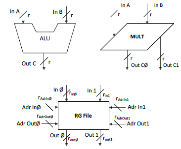
Figure 1: Functional modules of PE architecture
There are a great number of various PE's architectures based on the sets of modules similar to the mentioned above. So we use the parameters Lh, Lt, Fmax and ![]() to estimate each PE.
to estimate each PE. ![]() , where Tmin is the shortest module output time interval;
, where Tmin is the shortest module output time interval; ![]() , where f is a clock frequency. Parameter
, where f is a clock frequency. Parameter ![]() is an estimate of data processing efficiency for PE.
is an estimate of data processing efficiency for PE.
Various structures of PE architectures were generated by means of computer simulation and each structure was estimated by four parameters mentioned above. Three of the most efficient PE architectures are shown on Figure 2.
The results of the comparison of these architectures:
- the architecture on the Figure 2a) performs basic operation with high efficiency but it is "strong" since other operations needed for navigation algorithms are performed with latency, for example c:= a . b (output delay);
- the architecture on the Figure 2b) is the "fastest" (it is very good for data flow applications) but it is too complicated and as well as the previous architecture has delay for simple operations, for example, c:=a + b. In addition a delay for adding grows if a number of data input channels increase;
- the architecture on the Figure 2c) represents compromise between Lh and Lt It provides the minimal time of basic operation processing, performs important operations (adding and multiplication) with maximal performance (as well as the architecture on the Figure 2a) and has the minimal gate number (Lh).
There is no architecture with ![]() = 100% because of N+ = M – 1<< Nx = (N – 1)M, where N+ and Nx are numbers of addition and multiplication needed for basic operation.
= 100% because of N+ = M – 1<< Nx = (N – 1)M, where N+ and Nx are numbers of addition and multiplication needed for basic operation.
Architectural parameters of considered PE are shown in Table 1
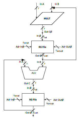
2a)
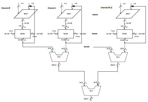
2b)
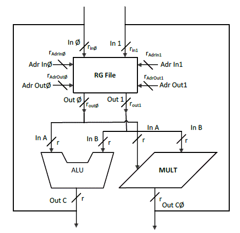
2c)
Figure 2: Some PE architectures

Table 1. Architectural parameters for some PE
The architecture on the Figure 2c) was chosen as the basic one.
3. PE DESIGN
Modules ALU, MULT and RGF were developed on the base of standard CMOS technology used for airand space-born applications (not less than 90 nm). Module ALU. It performs arithmetic and logical operations on 64-bit data. In addition ALU realizes all kinds of shifts for sign numbers; r-bit shift needs not more than one cycle. The structure of ALU is shown on Figure 3.
Flag Register (RegF) is used for storing of different signs of operations. RegF is 64-bit subdivided into four zones: shift signs, arithmetic operations signs, auxiliary signs (for example SLT = N ![]() V, where N is a sign of negative number and V is a sign of overflow) and reserve zone
V, where N is a sign of negative number and V is a sign of overflow) and reserve zone
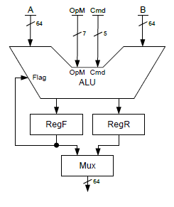
Figure 3: Module ALU
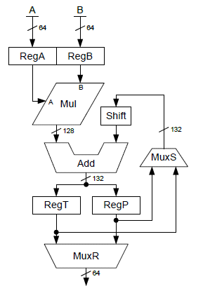
Figure 4: Module MULT
The Register of Operation Result (RegR) is needed for store of the last ALU operation. The number of ALU operations is 32. Time for each ALU operation is one cycle.
Module MULT. It performs following operations: usual multiplication of the 2's complement numbers, MAC, multiplication with 64-bit shift and multiplication with rounding. Structure of MULT is shown on the Figure 4. Time for each operation of the MULT is one cycle.
Module RGF. This module is four-port RAM with independent addressing of each port. Size of RGF is 6464 bit. Module RGF permits writing or reading four data flows concurrently. This feature of RGF provides maximum performance of PE in generally.
IP-Core. Core represents PE, consisting of three modules (ALU, MULT and RGF). Each operation of сore has execution time not more than one cycle so its architecture is RISC. The core is based on VLIW architecture with 132-bit instruction. This instruction consists of following main fields:
- Operation control. It generates opcodes for ALU and multiplier and necessary signs ("0", "SIGN", "OWFL").
- Microprogramming execution control. It provides an address of a "next" microinstruction that is used for branching.
- Interruption control. It provides analysis of the external break requests and reaction of the core.
- Microprogramming constants. This field contains constants that can be loaded into register file.
- Control of the internal data bus. By means of this field execution modules (ALU, MULT), RGF and external data channels are connected to internal data bus.
- RGF control. It generates addresses and control signals for four-port RGF. RGF contains array of 64x64 registers.
- Timer control. It provides initializations and stops of the timer as well as data writing to it from registers or memory. Timer has 32 bits.
- Memory control. It is needed for the control of the address counter.
Each instruction of the core is performed over one cycle. The set of instructions contains the following groups of instructions:
- Arithmetic instructions for 64-bit fixed point data ADD, SUBT, MULT and MAC.
- Logical operations on 64-bit, 32-bit binary data.
- Shifting and normalization.
The final goal of our project is IP-core of the VLSI; today we have completed FPGA project. It consists of two parts that are core and environment for debugging. For development and compilation we have used Verilog. Debugging was implemented by means of IDE QuartusII. In addition our team has used the synthesized processor core Nios II.
The hardware model of the core and the debug environment were developed on the base of FPGA Altera Cyclone® IV 4CE115 mounted on the debug card Terasic DE2-115 with f = 40 MHz. Both the core and the debug environment take not more than 83 percent of FPGA LUTs. Application of this core to SINS allows implementing basic SINS algorithms with updating interval about 0.3 ms. Equivalent performance is about 108 operations per second.
Real programming of Savage algorithms on processors with MIPS and Garvard architectures and core described above has shown that VLIW-RISC core requires from 2 to 4 times less than MIPS and Garvard. This results from orientation of the core architecture on effective realization of SINS algorithms.
The structure of FPGA-based environment for debugging of the hard and soft is shown on Figure 5. The core is highlighting by the dotted line.
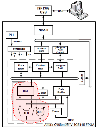
Figure 4: VLIW-RISC IP-core and FPGA-based system for research and development of FOP SINS.
4. CONCLUSION
The processor core with VLIW-RISC 64-bit architecture was developed on the base of analysis of the one class of algorithm for inertial navigation. The effective computational modules were developed as the base for that core. Today this core is implemented as a part of FPGA Altera Cyclone® IV 4CE115. Optimization of the architecture results in full volume of hardware of the core and debug environment not more than 83 percent of FPGA LUTs. The second stage of our study will focus on ASIC.
5. RFERENCES
1. P.G. Savage. Strapdown System Computational Elements. Advances in Navigation Sensors and Integration Technology. RTO Lecture Series 232 (2004) Pre-Prints. May 27-28, 2004, Saint Petersburg.
2. L. Belsky, L. Vodicheva, O. Maslova, N. Lookin, Ig. Ponomarev, L. Tolstikhina, A. Filimonov, A. Busygin. A Small Size Precise SINS for High Maneuvering Moving Vehicles: Optimal Design and Practical Results. The 10th Saint-Petersburg International Conference on Integrated Navigation Systems, May 26-28, 2003, Saint Pe-tersburg.
Related Semiconductor IP
- Voltage and Temperature Sensor with integrated ADC - GlobalFoundries® 22FDX®
- 8MHz / 40MHz Pierce Oscillator - X-FAB XT018-0.18µm
- UCIe RX Interface
- Very Low Latency BCH Codec
- 5G-NTN Modem IP for Satellite User Terminals
Related Articles
- CAST Provides a Functional Safety RISC-V Processor IP for Microchip FPGAs
- Interstellar: Fully Partitioned and Efficient Security Monitoring Hardware Near a Processor Core for Protecting Systems against Attacks on Privileged Software
- SoC Test and Verification -> Assertions speed processor core verification
- MPEG-4 is accelerated and footprint reduced by use of a configurable processor core
Latest Articles
- SNAP-V: A RISC-V SoC with Configurable Neuromorphic Acceleration for Small-Scale Spiking Neural Networks
- An FPGA Implementation of Displacement Vector Search for Intra Pattern Copy in JPEG XS
- A Persistent-State Dataflow Accelerator for Memory-Bound Linear Attention Decode on FPGA
- VMXDOTP: A RISC-V Vector ISA Extension for Efficient Microscaling (MX) Format Acceleration
- PDF: PUF-based DNN Fingerprinting for Knowledge Distillation Traceability