Integrated Power Management, Leakage Control and Process Compensation Technology for Advanced Processes
By Dan Hillman, Transmeta Corp
Santa Clara, CA, USA
Abstract :
Advanced process technologies, such as 90nm, 65nm, 45nm and below, present significant power management challenges for high performance semiconductors.
Chip designers face increasing challenges in meeting performance and power goals. Advanced process technologies tuned for high performance semiconductors are implemented at the expense of substantial increases in active, average and standby power. Exponential growth in transistor leakage in these advanced processes widens the performance-power trade-off gap. Increasing transistor leakage, coupled with manufacturing variations, can result in wide distributions of minimum frequency and maximum power consumption results across chips. Chip designers are challenged to choose between standard processes to meet performance goals or low power processes to meet power goals.
This paper describes a unique suite of power management, leakage control and process compensation technology geared towards reducing power while optimizing performance. This integrated solution, including advanced algorithms, innovative circuits, unique devices and structures, software and manufacturing optimization methods, will be discussed. Silicon performance results will be reported.
Process Variations
Most design parameters that chip designers use are subject to a statistical variation, often resembling a normal (Gaussian) distribution. Semiconductor foundries provide parameters to chip designers to account for the statistical variations in their process, outlining the fastest and slowest transistor speeds in their process. Because there are two types of transistors in a CMOS process, the NMOS and PMOS transistors, foundries provide the values that form the four different corners and the center of a “SPICE Box” – denoted as fast-fast (FF), slow-slow (SS), fast-slow (FS), slow-fast (SF) and typical-typical (TT). A “SPICE Box” is illustrated in Figure 1. The impact on design leakage from the SS corner to the FF corner can be as much as 30:1.
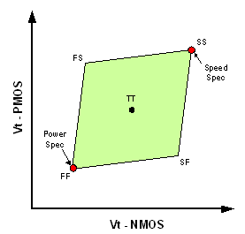
Figure 1 – SPICE Box
Typically, parts designed for a fixed supply voltage and manufactured in the FF corner will have the highest frequency, have the most leakage (which sets the power specification) and provide the best performance. Similarly, parts manufactured in the SS corner will have the slowest performance (which sets the speed specification), have the least leakage and consume the least power.
Tightening the SPICE Box
Threshold voltage control can be achieved with a technique called body bias, also known as back bias or substrate bias. Body bias leverages a MOS transistor effect known as the ‘body effect’ to control Vt. As shown in Figure 2, the application of reverse body bias raises the Vt of the NMOS and PMOS transistors. The overall effect is to move the FF, FS, and SF points of the SPICE box and move them closer to the SS corner. This technique works on all Vt variations, low, standard and high, within a process node. This can be a post-process adjustment performed on packaged parts, or alternately a new library corner could be made at the FF corner with bias applied. In the latter case, the chip designer can take advantage of the improved SPICE box to realize a lower power design. For example, a 30:1 leakage variation can be reduced to 5:1 with the use of reverse body bias. The amount of Vt change, and therefore leakage reduction, resulting from reverse body bias is called tunability. The amount of tunability in each process is different.
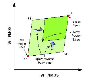
Figure 2 – Tightening the SPICE Box with reverse body bias
LongRun2TM Power Management
Transmeta’s LongRun2 technology addresses the growth in leakage power and increased manufacturing variations challenges with a comprehensive solution that includes: hard IP advanced algorithms, innovative circuits and manufacturing optimization methods.
LongRun2 technology is a suite of IP based post-wafer-processing compensation, power management, and leakage control technologies that optimize leakage power and diminish process variations in designs. LongRun2 offers a solution to meet performance, dynamic and static power. LongRun2 technology can dynamically adjust Vt and Vdd to selectively reduce the effects of process variation to improve yield, reduce worst case power at a given frequency, or increase performance within given power limits
Figure 3 shows a graph with Vt distribution that illustrate two yield curves – one without threshold voltage control (No LongRun2), and one with threshold voltage control (LongRun2). With reverse body bias the threshold voltage is increased which lowers the leakage power and performance of the circuit. The curve shows the shift in Vt distribution with LongRun2.
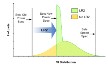
Figure 3 – Improved Vt Distribution
Figure 3 shows the static power reduction as a result of the Vt shift from LongRun2. The LongRun2 curves show the improved parts distribution to a newer lower power specification and tighter distribution. Note that the threshold shift is not large enough to affect the circuit performance.
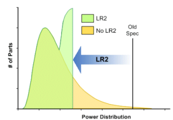
Figure 3 – Improved Power Specification
Optimizing Active Power
Active power is a combination of both dynamic power and leakage (static) power. At first examination, it may seem that the obvious solution to minimize active power is to minimize or eliminate leakage power. However, a deeper analysis shows that eliminating leakage power does not lead to minimizing total power. The interaction between the supply voltage, threshold voltage, frequency, and other design (logic depth) and process variables results in an active power curve illustrated in Figure 4.
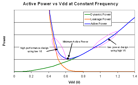
Figure 4 – Consumption vs. Threshold Voltage and Supply Voltage
Figure 4 illustrates dynamic power, leakage power and active power for a device at a fixed frequency. The x-axis represents the supply voltage required maintain the device at a fixed frequency, while allowing the threshold voltage to vary to meet the fixed frequency specification. The active power curve is the dynamic power curve plus the leakage power curve. As shown in the figure, the minimum active power is at the bottom of the active power curve. To better understand Figure 4, consider the following two examples:
Example 1:
Assume a high performance design utilizes low threshold voltage transistors to meet a frequency specification. With low threshold voltage transistors, the transistors switch faster and therefore a lower supply voltage can be used to operate the device at the desired frequency. In Figure 4, such a device would be to the left of the minimum active power point, denoted as ‘high performance design using low Vt’ in the figure. The device has high leakage power because it uses low threshold voltage transistors, but the dynamic power component is fairly low because a lower supply voltage is used. For this case, increasing the transistor’s threshold results in a substantial leakage power reduction. At the same time, increasing the supply voltage will slightly increase the active power consumption, but by a small amount compared to the leakage power reduction.
Example 2:
In a contrasting design, assume high threshold voltage transistors are utilized for a low power design. The high threshold voltage transistors will switch slower and require a higher supply voltage in order to meet the desired frequency. In Figure 4, the device would be to the right of the minimum active power point, denoted as ‘low power design using high Vt’ in the figure. The device will have fairly low leakage power because high threshold voltage transistors are used, but the dynamic power will be high because a higher supply voltage is required to meet the frequency specification. For chip designs in this region, reducing the threshold voltage results in a slight leakage power increase. However, with a lower threshold voltage, a lower supply voltage can be used. A lower supply voltage decreases the active power consumption by a larger amount than the increase in leakage power.
An obvious question is, “why not have the semiconductor foundry target the process to produce the ideal threshold voltage for the semiconductor device versus implementing threshold voltage control?” Manufacturing, temperature, and power supply variations make it impossible to achieve the minimum active power point without another dimension of control. In addition, depending on the logic depth, frequency of operation, library design, etc. each chip design would require a different threshold voltage.
Production Proven Technology
The LongRun2 technology has been proven to work effectively in volume production on NEC’s M2 mobile phone chip. LongRun2 as well as a variety of other power reduction techniques were used on this chip. By using the LongRun2 technology, NEC was able to increase performance on their M2 chip while maintaining the same power as the previous generation. NEC used low threshold transistors to increase performance and used back bias to reduce worst case leakage to an acceptable level. This is illustrated with NEC’s slide in Figure 5. This original version of this slide was in Japanese and has been translated to English for this white paper. Also see NEC’s press release at http://www.necel.com/news/en/archive/0707/0401.html.
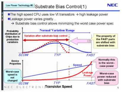
Figure 5 – Slide from NEC’s M2 presentation
Transmeta’s Efficeon microprocessor implemented LongRun2 to reduce worst case total power by 2.6 times without affecting speed.
LongRun2 technology has been licensed by Fujitsu, Intel, NEC, NVIDIA, Sony, and Toshiba.
LongRun2 IP
Transmeta has silicon-proven hard IP available to implement LongRun2 on SoC type designs. The IP consists of three blocks: Monitor Circuits, Controller and Bias Voltage Generator shown in Figure 6. The Monitor Circuits are ring oscillators whose frequency is dependent upon the circuit performance (speed), NMOS transistor leakage and PMOS transistor leakage. The Controller senses these frequencies and adjusts VDD, P-Well Voltage (VPW), and N-Well Voltage (VNW) to minimize power while maintaining the performance required for desired operation.
Transmeta has experience integrating LongRun2 technology into designs for production. Integration Guide and Product Engineering Application Notes are available to assist in LongRun2’s design and productization. The Integration Guide provides an EDA flow and guidance on how to easily handle unaffected analog and IO circuits. The Product Engineering Application Note instructs how to calibrate the monitor circuits to the design’s performance and how to determine the programmed value of the fuses. In production, the fuses provide the target settings for the monitor circuits so that the controller can achieve minimum active power. Fuses, one-time-programmable (OTP) devices, are generally available off-the-shelf for most foundry processes.
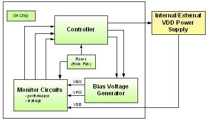
Figure 6 – LongRun2 IP
Dramatic Power Reduction
Transmeta’s LongRun2 technology provides a set of solutions to reduce variation across a distribution of parts which can improve the power specification, performance, yield, and reduce costs. Results will vary according to the design and how well the process works with LongRun2. The table below shows logic leakage reduction for a sample of process sizes.
| Process | Leakage Reduction | Comment |
| 90 Generic (std transistor) | 92% | tuned for LongRun2 |
| 65 Generic (std transistor) | 62% | standard process |
| 45 Generic (std transistor) | 68% | standard process |
The advantage of LongRun2 over other low power techniques is that it not only reduces power but also decreases the effects of process variations through post-process corrections. By reducing the effects of processes variability, the design specification can be tightened to achieve higher yield and lower power more effectively than with pre-process techniques. Other power reduction techniques are pre-process techniques only and do not address the process variation issue.
Related Semiconductor IP
- NPU IP Core for Mobile
- MSP7-32 MACsec IP core for FPGA or ASIC
- UHF RFID tag IP with 3.6kBit EEPROM and -18dBm sensitivity
- NPU IP Core for Edge
- Specialized Video Processing NPU IP
Related White Papers
- Keeping leakage current under control
- Take control of design data management
- Standardizing data interchanges among design tools in the ECU development process: Pt. 1 - Models, formats, and data management
- Beat power management challenges in advanced LTE smartphones
Latest White Papers
- Ramping Up Open-Source RISC-V Cores: Assessing the Energy Efficiency of Superscalar, Out-of-Order Execution
- Transition Fixes in 3nm Multi-Voltage SoC Design
- CXL Topology-Aware and Expander-Driven Prefetching: Unlocking SSD Performance
- Breaking the Memory Bandwidth Boundary. GDDR7 IP Design Challenges & Solutions
- Automating NoC Design to Tackle Rising SoC Complexity