MIPI M-PHY takes center stage
By Ashraf Takla and George Brocklehurst
The curtain is up and the M-PHY specification is taking center stage, positioned to handle the many different roles required for a faster, more reliable, physical interface layer (PHY Layer) on mobile devices.
The script for the M-PHY specification was written inside the MIPI (Mobile Industry Processor Interface) Alliance by a working group made up of member companies, and set up to expand the capabilities of mobile devices by defining interface standards that will revolutionize the capabilities of the coming generations of mobile products. Faced with an explosion of mobile multimedia devices, with an ever increasing demand for faster throughput, the mobile industry, through the MIPI Alliance, has defined the ultimate PHY, one capable enough to handle the demands of mobile devices and seemingly capable of moving into several other key application areas as the PHY of choice.
MIPI and the M-PHY
The M-PHY specification is an essential part of the MIPI Alliance’s vision for new and more capable high-speed interfaces on mobile devices. Members identified early the need for a serial interface to support the ever increasing data bandwidth requirements of mobile devices. Now, pressed even further by the explosion of digital content in video, social media exchanges, and cloud computing, mobile devices require a faster physical layer interface, like the M-PHY, to remain a step ahead of the data transfer requirements necessary to give consumers the on-device response they need. Fuelled by the success of the other MIPI Standards now being deployed, the M-PHY specification is gaining momentum as it moves toward final approval as the newest MIPI specification. The MIPI D-PHY, a source synchronous interface that is currently handling the interfaces between the application processor chip and the camera or display in a mobile device, has been especially successful. Even though the D-PHY is a capable interface, its synchronous nature has speed limitations (1 Gigabit per second) that prevent it from handling the demands for higher data transfer rates. The industry requires a more powerful PHY, one that offers asynchronous data transmission and addresses the speed and signal integrity issues of high-speed chip-to-chip connections within an increasingly EMI (Electro-Magnetic Interference) sensitive environment compounded by tighter form factors, while continuing to minimize power dissipation.
drloginrequired
The M-PHY plays many roles
Just like a versatile star, the M-PHY interface is talented enough to play many roles. When first envisioned, it handled the set of specifications already defined or in the process of being defined inside MIPI. Those specifications included the Camera Serial Interface (CSI), the Display Serial Interface (DSI), and a Universal Protocol (UniPro). The CSI and DSI specifications are easily understood: they define the protocol interfaces between the application processor and a camera or a display. UniPro (Universal Protocol) is a comprehensive specification meant to act as a universal chip-to-chip protocol, providing a common tunnel for other protocols. The M-PHY interface is designed as the primary physical interface (PHY layer) for the UniPro specification. The M-PHY specification has two signalling schemes, supporting both self clocking and embedded clocking. Additionally it runs at both lower and higher speeds. The high-speed communication option makes the M-PHY interface the perfect vehicle for UniPro offering speed, power and economy.
The first evidence of the M-PHY interface versatility emerged when the DigRFSM Alliance was assimilated into MIPI. The DigRF Alliance had defined a specification between the Baseband (BBIC) and the RF chip (RFIC) for mobile platforms. This new specification describes the logical, electrical and timing characteristics of the digital BBIC to RFIC interface. Accepting the role as the new physical interface is the M-PHY.
The M-PHY interface was further recognized by JEDEC as an ideal physical layer for its highly anticipated Universal Flash Storage (UFS) specification, defining a high-level interface that standardizes connectivity in an extensive range of diverse, non-volatile memory solutions currently being developed within the JC-64 Committee on Flash Memory Modules. The M-PHY is the perfect player for the PHY layer specification.
Building on this successful start, another subcommittee within JEDEC, the Low Power Memory J42.6 subcommittee, is also considering the M-PHY for yet another role as the Physical Layer for “future Mobile”.
The M-PHY specification, when finalized, will provide a physical layer that shall always be used in combination with a higher layer MIPI specification that references it. Any other use of the M-PHY specification is strictly prohibited, unless approved in advance by the MIPI Board of Directors.
The Character of the M-PHY
The M-PHY is defined as a serial link. The overall objectives fall into this general requirements list:
- Low pin count: all control signalling handled in-band across the interface
- Supports both electrical and optical interfaces using low complexity electro-optical signal conversion
- Optical friendly electrical specification (sufficient timing flexibility, DC balanced coding scheme, etc)
- Optimized for short distance (<10cm) but suitable for long-distance (m)
- Huge range of speed requirements: ~10Mbps to ~6Gbps
- Power efficient throughput adaptation using burst-mode
- Clocking: shared or non-shared reference clocks
- Independent of foundry process
- EMI friendly
- Multiple transmission modes for better power efficiency
- Multiple transmission speed ranges/rates for varied application needs and for mitigation of interference problems
- Fixed transmission rates for high-speed mode but flexible for low-speed modes within specified ranges
- Multiple power saving modes, where power consumption can be traded-off against recovery time
- Symbol coding (8b/10b) for spectral conditioning, clock recovery, and in-band control options for both PHY and Protocol level
- Configurability to reduce cost and tuneable for best performance
Since the M-PHY is meant to replace the D-PHY in applications that require higher throughput, systems designers will have a choice as to which physical interface to use. Table 1 highlights the differences between the D-PHY and M-PHY, and Figure 1 shows the location of the camera /and display subsystems linked by either the D-PHY or M-PHY interconnections.
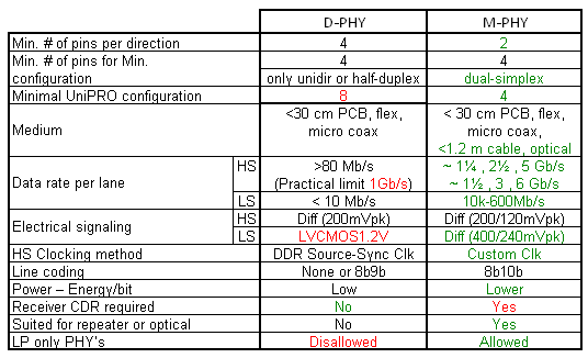
Table 1: Comparison of the characteristics of the MIPI’s D-PHY and M-PHY (Source: Den Besten, Gerrit of NXP)
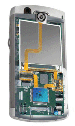
Figure 1: Inside of a mobile phone showing an example of MIPI connections between the application processor and camera and display subsystems. Connections made using a D-PHY or M-PHY (source: Mixel, Inc.)
The Stage and Script
The basic architecture of an M-PHY system is shown in Figure 2. Each LINK is made up of two SUBLINKs, containing one or more LANEs. A LANE is a unidirectional point-to-point differential serial connection between PINs, called a LINE, and connects an M-PHY transmitter and an M-PHY receiver. LANEs running in the same direction constitute a SUBLINK. Two SUBLINKs running in opposite directions, plus the additional management function, complete a LINK. Thus, the operation of the M-PHY interface is completely defined in the context of a protocol definition like DSI, CSI, UniPro, or DigRF which manage the LANE.
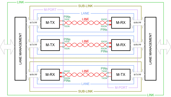
Figure 2: Architecture of the M-PHY LINK, made up of a LINE, LANE, and SUBLINKs and LANE Management (Source: MIPI Alliance)
There are two fundamentally different types of M-PHY interfaces, denoted as Type-I and Type-II, depending on which signalling scheme is used. For low-speed operation, Type-I employs PWM (pulse width modulation) signalling, while a Type-II uses system-clock synchronous NRZ (non-return-to-zero) signalling. Type-II requires a shared reference clock between the two ends of the line. Type-I is able to operate with independent local clock references on each side of the link. Type-I and Type-II are not interoperable, but implementations may support both types of in order to enable hardware reuse, so one M-PHY specifications can service multiple applications and connections inside a mobile device.
The two modes are illustrated in Figure 3. For PWM signalling (Type-I), there are multiple GEARs (they can switch like gears in a transmission) to cover different speed ranges. The default (mandatory) GEAR for Type-I is PWM-G1, ranging from 3 to 9 Mbps. There are six GEARs with incremental 2x higher speed ranges (PWM-G2 to G7), and one GEAR below the default speed range (PWM-G0). This GEAR-based architecture and the modulation scheme enable an M-PHY specification to optimally target data rates and power dissipation based on system requirements. The M-PHY interface can optionally support a high-speed mode (HS-MODE). The HS-MODE includes a default GEAR (HS-G1) and two optional GEARs (HS-G2 and HS-G3) at incremental 2x higher rates. For any given supported HS GEAR, all lower HS GEARs must always be supported e.g. support for HS-G3 alone is not allowed. Each GEAR includes two baud rates for EMI mitigation reasons, e.g. HS-G1 supports 1.25Gbps and 1.45Gbps. This is especially useful for supporting one handset sold in two geographical regions, which have different base-band frequencies; if one region with a particular base-band frequency suffers beating interference from PHY EMI the alternate rate may be selected. The G2 and G3 GEARS would operate at 2.5Gbps and 5Gbps respectively. Type-II uses a shared reference clock and thus does not require clock recovery. Between the architecture and the clocking options, the M-PHY specification enables the construction of a very versatile set of PHY operations that can target many different LINK requirements. The M-PHY definition is a complete “script”, in specification form, ready for “staging”, in silicon, and capable of handling the speed and power requirements of the next generation of mobile devices.
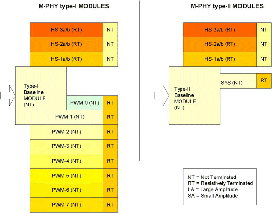
Figure 3: M-PHY Type-I and Type-II Clocking Architectures (Source: MIPI Alliance)
Working the Media
The motivation for specifying a more capable PHY not only has to do with adding exciting new features, but also with improving the reliability of mobile devices. Connecting two sides of a clamshell phone, requires interconnect flexible enough to withstand mechanical stressors, at transfer speeds high enough to satisfy the applications requirements, and signal quality good enough to ensure reliable reception. In addition, this PHY must dissipate minimal power and contribute little EMI. The connector medium used has historically been thin (< ~1 mm) copper wiring. As few wires as possible should cross the connection so that signal integrity problems remain in check without constraining the handset design, hence the strong preference for high speed serial interface.
Optical links offer robustness and mechanical flexibility, along with superior EMI and noise immunity. Some mobile devices have complex hinge (flip-side-twist) mechanicals. These hinges give viewers control over their viewing angle, which is very important when the display is smaller, and when it’s necessary to reduce eye and neck stress. One example of a complex two axis movement is shown in Figure 4, where the first access acts like a flip phone and the second allows adjustment of the display viewing angle. The data rates across these hinges and the susceptibility to mechanical failure limits the number of copper connections that cross the hinge and the materials that can be used to maintain reliability.
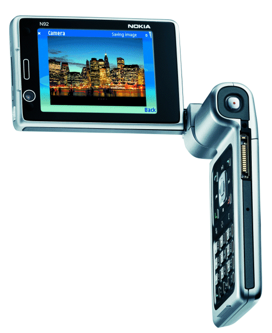
Figure 4: Advanced mobile devices have axis movements that add mechanical stress to interconnects between the display and processor (Source: Nokia Corporation)
Optical interconnect allows the rules to be re-written and decouples system architectures from handset form-factor design, allowing a common platform to be used across many handset models regardless of hinges, features, and physical attributes.
Traditionally the optical components have been viewed as overhead in terms of power and cost, and to a large extent this is true, since portable consumer electronics cannot tolerate an extra couple of dollars on the BOM or some additional milliwatts. However with serialization and the resulting increase in data rates, copper solutions become comparable in cost (@ ~3Gbps) and don’t offer the ancillary benefits of optical. Furthermore optical offers improvement in the $/Gbps and mW/Gbps ratios as the data rate goes up offering a forward looking roadmap where copper would likely follow a restrictive trend. Add to this the impact that a small fraction of the large consumer volume will have on the cost models within the optical PHY industry, which currently operates on relatively low volumes by comparison, and you will likely see accelerated optical module price reduction and improved performance.
The MIPI PHY Working Group anticipated using an optical medium to mitigate these growing issues, setting up an Optical Sub-Group to define an Optical Media Converter (OMC), that converts electrical signals from an M-PHY Transmit (M-TX) into optical signals (light waves), transports the signals across a medium such as a Plastic Optical Fibre (POF), and converts the optical signals back into electrical signals that an M-PHY Receiver (M-RX) can receive. An OMC is considered to be like a “module”, an inseparable unit, consisting of an optical transmitter (O-TX), an optical receiver (O-RX), each with appropriate photonics, and an optical wave guide. Since OMC is one unit, interoperability between optical modules is not required, and thus the optical domain is not specified within MIPI.
These “modules” are well understood in the high speed optical markets like SONET/SDH and as part of the IEEE Ethernet, Fibre Channel, and OIF-CEI specifications. The module and its electrical connections are illustrated in Figure 5.

Figure 5: MIPI’s Optical Media Converter Module defines an electrical-optical interface for Mobile Devices (Source: MIPI Alliance)
Furthermore, if these high-end video capture and display applications, and the subsystems that support them, dissipate more power, resulting in intolerable ground shifts across traditional copper interconnect, then optical interconnect is even more desirable.
Whether copper or optical fibre is used, the M-PHY specification defines a flexible architecture that allows the implementer to support high data rates at minimal power and cost. The challenging aspects of delivering high-definition streaming video; loading of gigabyte wide movies (from the Internet) in an “everyone, everywhere, seamless wireless connection to surrounding devices and services” will only come from an optimized chip-to-chip interface– like the M-PHY.
The Final Act
The final necessary ingredient for the successful deployment of the M-PHY specifications is a healthy ecosystem of companies that can develop, test, demonstrate interoperability, and deliver the M-PHY infrastructure to market. The collaboration between suppliers who can fill these roles is the final act in realizing the ultimate benefit of all the work done by so many contributors in the MIPI Alliance. One of the key components of a vibrant ecosystem, are the IP providers that can build and deliver the M-PHY subsystem so that rapid adoption can take place. The very nature that makes the M-PHY interface unique, namely its versatility, its many architectural options, and its ability to address many different applications, makes a one-size-fits-all IP approach a self-defeating proposition. This is different from other standards such as PCI Express, SATA, or DDR, where a single architecture can be ported to many process nodes to effectively address the requirements of thousands of customers. For the M-PHY to fulfill its potential of being an optimized solution for applications where power, area, and total cost are all parameters of paramount importance, a cookie-cutter approach will not do. Successful MIPI adopters will be those who can partner with an M-PHY IP vendor that can provide a shrink-wrapped, silicon-proven yet customizable, high quality differentiated IP at reasonable cost.
Mixel Inc. has already announced one of its M-PHY customers, Graphin CO. LTD. of Japan. Together the two companies plan to support the MIPI M-PHY ecosystem by building a “Golden M-PHY” IC to be used in Graphin’s evaluation systems. The same “Golden M-PHY” IC will be made available to support M-PHY interoperability and testing requirement of the MIPI ecosystem. Mixel is also collaborating with Nanotech Semiconductor, of the UK, which chairs the Optical M-PHY subgroup, to support the MIPI M-PHY optical ecosystem. Mixel employs what it dubs a “Legorithmic” approach, which enables it to effectively develop efficient, shrink-wrapped MIPI IP, based on its silicon-proven building blocks to meet the large set of M-PHY flavors that will be required for the variety of M-PHY applications.
Reference 1: ABI Research
About the Authors
 | Ashraf Takla is the President and CEO of Mixel Inc., which he founded in 1998. Before Mixel, Takla was Director of Mixed-Signal Design at Hitachi Micro Systems, and also worked at AMI and Sierra Semiconductors. Takla has 30 years of experience in analog and mixed-signal design, and holds 5 patents. Takla received his BSEE & MSEE degrees from San Diego State University. – www.mixel.com |
 | George Brocklehurst is the Marketing Director for Consumer for Nanotech Semiconductor Ltd since 2005 and currently holds two chairing roles within the MIPI Alliance; Vice Chair PHY WG and Chair Optical SG. Brocklehurst has 10 years product/market development experience in the semiconductor industry in consumer and telecoms sectors and holds an MBA from Southampton Solent University and a BEng Electrical Eng degree from Southampton University - www.nanosemi.co.uk |
Acknowledgement
The authors would like to acknowledge the contribution of all MIPI Alliance members who participated in the creation of the M-PHY material included in this Article. Use of such material was approved by the MIPI Alliance Board of Directors.
Related Semiconductor IP
- MIPI M-PHY
- MIPI M-PHY IP
- MIPI M-PHY Verification IP
- Simulation VIP for MIPI M-PHY
- MIPI MPHY Verification IP
Related White Papers
- Understand and perform testing for MIPI M-PHY compliance
- Addressing MIPI M-PHY connectivity challenges for more efficient testing
- RISC-VLIW IP Core for the Airborn Navigation Functional Oriented Processor
- Secure SOC for Security Aware Applications
Latest White Papers
- Concealable physical unclonable functions using vertical NAND flash memory
- Ramping Up Open-Source RISC-V Cores: Assessing the Energy Efficiency of Superscalar, Out-of-Order Execution
- Transition Fixes in 3nm Multi-Voltage SoC Design
- CXL Topology-Aware and Expander-Driven Prefetching: Unlocking SSD Performance
- Breaking the Memory Bandwidth Boundary. GDDR7 IP Design Challenges & Solutions