MIPI Drives Performance for Next-Generation Displays
By Mixel, Rambus, and Hardent
In late 2000, Nokia announced its iconic 3310 handset which featured an 84×48-pixel pure monochrome display. Seven years later, Apple unveiled its first iPhone with a 90mm (3.5”) screen and 320×480-pixel resolution (at 163 ppi). Cameras and high-quality displays quickly became the de-facto standard for smartphones by the mid-2000s. However, proprietary interface solutions for connecting cameras and displays to mobile processors lacked the standardization needed to make sense of the chaos of sourcing these components in a rapidly growing mobile phone market.
The Mobile Industry Processor Interface (MIPI®) Alliance was formed in 2003 to address the fragmentation in the essential video interface technologies for cameras and displays in phones. In later years, the alliance significantly expanded its scope to publish specifications covering physical layer, multimedia, chip-to-chip, control/data, and debug/trace and software. With its broader mission, “MIPI” became a name rather than an acronym for the MIPI Alliance.
Initially, MIPI competed with MDDI (Mobile Display Digital Interface) for the title of industry standard. Although there was a short-lived market for MDDI-to-MIPI bridge chips, the low power, low-latency, scalable performance of MIPI, combined with broader industry support, prevailed. Today more than a billion phones (1.7B in 2019) and 100 million tablets ship annually with MIPI- standardized technology for their cameras and displays.
In this white paper, we will explore the history of MIPI display technology, (DSI and DSI-2), MIPI display markets, and the emerging bandwidth gap given the performance requirements of next- generation displays.
MIPI Display Technology
DSI
The first iteration of MIPI’s Display Serial Interface (DSI) specification debuted in 2006. The specification – which defines the interface between the processor and display(s) – achieved widespread adoption. Along with its DSI-2 successor, DSI is the leading display interface used in smartphones, tablets, and laptop/tablets hybrids. It is also used by the automotive industry for dashboard displays and in-car infotainment systems, as well as in wearables, IoT, and AR/VR applications.
MIPI DSI, which utilizes the MIPI D-PHY physical layer, uses a command set defined in the MIPI Display Command Set (MIPI DCS). It also incorporates the Display Stream Compression (DSC) Standard from the Video Electronics Standards Association (VESA).
DSI-2
Initially published in January 2016, MIPI DSI-2 supports ultra-high definition (4K and 8K) resolution demanded by new and future mobile displays. It specifies the physical link between the chip and display in devices such as smartphones, tablets, AR/VR headsets and connected cars. In addition to the MIPI D-PHY, DSI-2 supports use of MIPI C-PHY as the physical layer.
MIPI DSI-2 v1.1 incorporates two VESA video compression standards in its transport layer: VESA DSC and VESA VDC-M. This means designers can now select a codec that gives them tremendous flexibility in resolution, bandwidth and power requirements. VESA introduced the first DSC standard in 2014 and it quickly became the industry standard for data compression across the display interface. DSC was the first to offer a low latency, low complexity codec expressly designed for this purpose.
MIPI Display Markets
As its capabilities have grown, MIPI display technology has evolved to support far more than the basic requirements of mobile phones. The DSI-2 protocol supports ultra-high definition displays up to 8K resolution. In the sections below, we take a closer look at how MIPI is helping to enable the trio of applications-– IoT, Automotive, and AR/VR – highlighted earlier.
IoT
Beyond bandwidth, MIPI offers multiple technical benefits for IoT applications including low power consumption and low EMI. With regards to low power, MIPI specifications enable an IoT device to be powered from a battery over many years or draw power from renewable sources such as solar or wind energy. In terms of low EMI, MIPI specifications help reduce EMI through a combination of factors such as low-voltage swings on high-speed physical layers and slew rate control. This provides developers with the flexibility to adjust the EMI profile of the physical layer interface to meet the EMI requirements of the end device.
Automotive
Today’s vehicles are brimming with a plethora of advanced cameras, sensors and displays. To be sure, ADAS is used to enable park assist, driver monitoring, blind spot detection, night vision, and vehicle security systems. In addition, cockpits and infotainment systems feature multiple high- resolution displays that utilize MIPI interconnects.
MIPI specifications found in vehicles today include CSI-2, DSI-2, C-PHY, and D-PHY. Moreover, the MIPI Alliance has defined the MIPI A-PHY, a physical layer specification designed for ADAS and autonomous driving systems (ADS). The A-PHY also serves additional surround sensor applications in automobiles (e.g., for displays, and cameras.) While most MIPI specifications are designed for shorter reaches for use within mobile devices, A-PHY is capable of reaching up to 15 meters in demanding automotive environments. A-PHY v1.0 supports up to 16 Gbps, with a roadmap to 24 Gbps, 48 Gbps and beyond.
AR/VR
MIPI-based cameras, displays, and sensors are all playing a significant role in the continued advancement of AR/VR devices that demand higher pixel density (ppi), pixel resolution (bpc), and frame rates. As bandwidth demand increases, MIPI offers product designers a reliable specification that interfaces with the components to deliver the required throughput while minimizing pin count, energy consumption, and EMI. More specifically, AR/VR designers use CSI-2 to interconnect cameras and high-end SoCs, and MIPI DSI to support multiple displays (one for each eye).
The Growing Bandwidth Gap
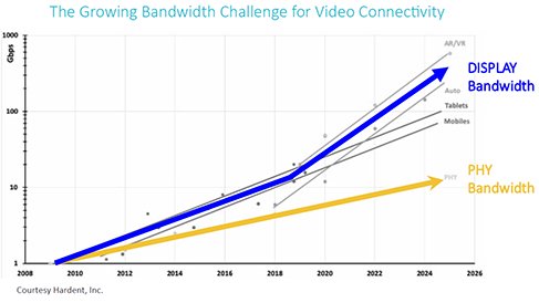
Mobile display requirements have advanced significantly over the past few years, with high-end smartphones now delivering 120 frames per second (fps) to support gaming and 4K video. OLED adoption by major smartphone manufacturers has made 100 Mbit frame buffers quite common. In the highly competitive mobile phone market, where display resolution is a key selling feature, it’s perhaps not surprising that display bandwidths have increased by a factor of 23x in the past decade. Meanwhile, the bandwidth capabilities of display interfaces have only increased by a factor of four to five.

The industry has responded by deploying visually lossless compression to close the gap. Visually lossless compression is supported by Display Stream Compression (DSC) algorithms and encoders (such as those provided by Hardent), which are typically integrated into mobile application processors. On the flip side, DSC decoders are integrated into the DDIC chips found in the display module of mobile phones.

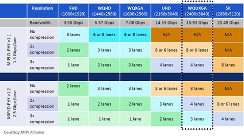
As the table above illustrates, compression allows device designers to minimize the number of MIPI D-PHY lanes. For WQUXGA (2400x3840) resolution requiring 15.93 Gbps, MIPI D-PHY v1.1 (1.5 Gbps/lane) can achieve this resolution with 4 lanes at 3x compression (versus not at all with no compression). With MIPI D-PHY v1.2 (2.5 Gbps/lane) can deliver WQUXGA with just 3 lanes using 3x compression.
In addition to minimizing the number of MIPI D-PHY lanes, DSC reduces the memory buffer and bandwidth demands, thereby enabling smaller footprints, power savings and reduced cost. The VESA DSC algorithm, for example, is used across a wide range of devices, including smartphones, tablets, GPUs, AR/VR head-mounted displays, in-car video systems, 8K TVs and high-resolution monitors. The VESA DSC algorithm offers compression as low as 8 bpp without any perceptible differences, along with extremely low latency performance. DSC is a lightweight codec that requires no external DDR storage. Only a single line of pixel storage (SRAM), plus rate buffer is needed.
Integrated MIPI DSI-2 VESA DSC IP Solution
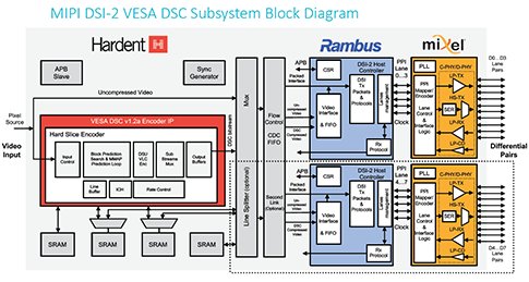
Mixel, Rambus and Hardent offer a fully integrated state-of-the-art solution for next generation display applications requiring high bandwidth and excellent power efficiency. This integrated solution brings together the IP of the three MIPI Alliance member companies enabling rapid deployment of mobile, AR/VR and automotive displays leveraging MIPI DSI-2 interface and VESA DSC compression technology.
The solution consists of:
- MIPI C-PHY/D-PHY Combo (Mixel)
- DSI-2 Controller (Rambus)
- VESA DSC (Hardent)
This subsystem achieves excellent effective bandwidth utilizing one or two DSI-2 links with MIPI D-PHY or MIPI C-PHY and VESA DSC visually lossless video compression. It sets a new benchmark for performance, ease of implementation, and time to market using proven, broadly adopted IP.

Highlights
- Dual or single channel MIPI DSI-2 Transmitter with VESA DSC including:
- Mixel MIPI C-PHY/D-PHY Combo (2 instances with dual channel)
- Rambus DSI-2 Host Controller (2 instances with dual channel)
- Hardent DSC v1.2a Encoder IP
- Uncompressed and DSC compressed video transmission supported across one or two links
- Supports asynchronous pixel source (from DMA) or synchronous pixel source (parallel video)
- Low power features
- SRAM sharing to reduce silicon area
- Host (Tx) and peripherals (Rx) versions available
- Integrated solution available from Mixel, or the three IP cores can be licensed separately from Mixel, Rambus and Hardent
Conclusion
MIPI technology is critical to enabling the dramatic growth of the mobile phone market. The function and capabilities of MIPI interface solutions have grown apace. MIPI DSI-2 has become the leading display interface across a growing range of products including smartphones, AR/VR, IoT appliances and ADAS/autonomous vehicles.
As the application space has expanded, so too have the performance requirements. The demand for higher and higher bandwidth is rapidly outstripping the raw bandwidth improvements in the physical layer alone. The key to closing the gap and delivering the needed display bandwidth is bringing together MIPI DSI-2 interface and VESA DSC visually lossless compression technologies. MIPI Alliance partners, Mixel, Rambus and Hardent now offer an integrated subsystem that gives designers an easy to implement solution for next-generation display applications.
For more information, please visit:
Related Semiconductor IP
- MIPI CSI-2 IP
- MIPI C/D Combo PHY RX - GlobalFoundries 22FDX
- Controller for MIPI Soundwire
- MIPI DSI-2 RX Controller
- MIPI SoundWire Slave Controller 1.2
Related White Papers
- VESA Video Compression on MIPI DSI-2 Enables Next-Generation Display Applications
- Performance Evaluation of machine learning algorithms for cyber threat analysis SDN dataset
- Maximizing Performance & Reliability for Flash Applications with Synopsys xSPI Solution
- Boosting RISC-V SoC performance for AI and ML applications
Latest White Papers
- Breaking the Memory Bandwidth Boundary. GDDR7 IP Design Challenges & Solutions
- Automating NoC Design to Tackle Rising SoC Complexity
- Memory Prefetching Evaluation of Scientific Applications on a Modern HPC Arm-Based Processor
- Nine Compelling Reasons Why Menta eFPGA Is Essential for Achieving True Crypto Agility in Your ASIC or SoC
- CSR Management: Life Beyond Spreadsheets