Low Power Design for Testability
Miteshwar M. Patel (ASIC Engineer, eInfochips Ltd)
Nirav Nanavati (Tech Lead, eInfochips Ltd)
Abstract
Design for testability (DFT) and low power issues are very much related with each other. In this paper power reduction methodologies are discussed for a given design. Power management circuitries are developed to reduce functional power of the design. Power aware Scan Chains are implemented to create test environment which result into reduction in test power. Design for testability is applied to test power management circuits using Power Test Access Mechanism. Also few methods are discussed to implement DFT to test power management circuitry and improve test and fault coverage during ATPG.
Keywords: DFT (Design for testability), Low power, Power management circuitry, Unified power format, ATPG (Automatic test pattern generation).
1. Introduction
Low power issues are very much concern during this era of technology. As the technology tends to reduce its size, more and more complexities with power issues come into existence. Large Integrated circuits require an increasing amount of data to test them which increases testing time and tester memory. Power reduction is needed during functional mode and test mode of the design.
As integrated circuit feature size continues to shrink and portable devices grow, power consumption not only becomes one of the key issues to be considered during functional operation, but also has to be considered during manufacturing tests [1]. High power consumption during the functional operation implies:
- Higher design and manufacturing costs due to the extra effort to calibrate power grids in order to meet the power supply requirement.
- Higher system costs due to packaging and cooling requirements.
- Shorter device life cycle and lower device reliability.
- Shorter battery life for portable devices.
In real world mobile applications, it is essential to save power in parts of the chip that are not in use. Nowadays, chips integrate several systems on a single chip (SoC); each of these SoCs is also called intellectual property (IP). In order to save current consumption, each IP can move between power modes (power-off/power-on/sleep). Each IP is divided into power domains, and those power domains can be turned on and off as well, according to the power-mode. Memory and register values can be restored after being shut down (also called retention). There are isolation cells which keep the turned off IP outputs in a previously defined value, and this is how the shut-down IP does not corrupt other active IP functionality [2]. Our power-management test methodology test the functionality of all the power-management elements described above.
In this paper section 2 discuss power specification formats like UPF/CPF. It describes how basically power formats provides way to design power management circuitry to reduce functional power. Section 3 describes Power Management Circuitry and its functionality to reduce power in briefly. Section 4 discusses Design for testability, as creating power aware scan chains. The scan chains are created depending upon the power domains and Daisy chain approach to provide effective power aware scan chains. Section 5 consists of DFT synthesis flow and power management techniques. Power Test Access Mechanism is inserted during DFT insertion to improve controllability and observability of power management circuitry. And at last section 6 describes few methods applied to test power management circuitry to improve test and fault coverage during ATPG and creating test protocol accordingly.
2. Power Specification Formats
To guarantee high productivity within flows and interoperability between flows, a concise specification of structural power aspects is being standardized for EDA tools. Two competing format exist. One is CPF (for common power format) and the other is UPF (for unified power format).
UPF/ CPF power specification formats basically provides a way to describe the following specifications, unique to low power design techniques [3]:
- Voltage domains or blocks operating at different voltage levels with level shifters inserted at all domains.
- Power domains or blocks with a separate power supply that can be turned off.
- Multiple supply nets with different names and connections.
- Isolation logic, placed at the o/p of power domain which may remain powered on.
- Retention registers, which are flop to flop within an always on power domain, to retain state when the domain supply is shut off.
- Always on cells and paths for logic, this must remain powered on even when the domain supply is switched off.
- Power switches, which are large on-chip switching transistor to shut off the power to a power down.
Using this power formats power management circuitry is developed around the design to reduce functional and test power, following section describes each circuit in details.
3. Power Management Circuit
The power management scheme is built by the power architect of the SoC in order to reduce the current consumption of the chip. There are several common building blocks which are used by the power management architect, as will be described in the next sections.
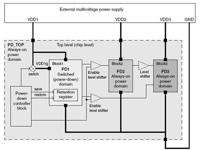
Figure 1: Functional power management circuitry
A. Clock Gating:
It’s a powerful technique to reduce the power consumption in a power-on domain through dynamically blocking the clock pulse to reach a set of sequential state elements. The clock gating is often hierarchically implemented in order to improve the flexibility to control the power consumption during functional operation.
B. Power Domains:
The design is created with multiple power domain blocks. Each block can be independently powered up or down by controlling the power switches used to gate the power supply connection to each power domain block.
C. Multiple supply voltages:
Depending upon operating conditions, different supply voltages are applied to different power domain blocks, and each power domain blocks are connected using level shifters.
D. Low Power Cell:
State Retention Cell: The ability of state retention registers (SRRs) to retain their state when the power domain is powered off needs to be validated during test. Conventional structural tests, if applied while a given power domain is forced on, cannot validate state retention since the domain is not powered off during the capture cycle.
Isolation Cell: The Isolation cells locate at the boundary of two power domains in order to isolate the power off and power on domain.
E. Power Switches:
To reduce power dissipation, especially leakage power dissipation introduced by shrinking process technologies, power switches are commonly used in modern low power designs. To enable the power gating functionality, different parts of the design are equipped with one or more power switches [4].
4. Creating power aware scan chains.
The main requirement to create power aware scan chains is that in a valid test mode the scan path, test clock and control signals should not traverse through OFF domains. In addition, any test signals that traverse through two power domains of different voltages should have the appropriate level shifters. The fan-out branches of the scan path and test signals that have sinks in the OFF power domains should have isolation logic for correct functional operation.
The simplest mechanism to create power aware scan chains is by partitioning the scan chains by power domain. If there are sufficient scan I/Os each power domain can be assigned its own dedicated scan I/Os, test clocks and control signals.
This ensures that each power domain has dedicated scan chains that are active in the power modes in which this domain is ON. This simplicity comes at a very high cost of test since the expensive tester resources are not fully utilized when one or more domains are OFF.
To more efficiently utilize the tester resources the full tester bandwidth needs to be utilized in every test mode. This requires that the test pin configuration is constant in every test mode.
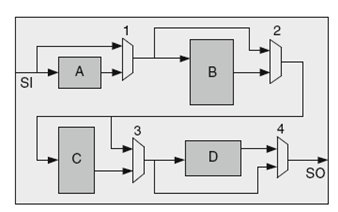
Figure 2: Power Aware Daisy Chain scan path.
One approach that has been implemented in our power aware methodology is a Daisy Chain approach which ensures that the every scan I/O pin is fully utilized. Furthermore the scan chains remains balanced across the various test mode.
Daisy-chain implementation along with bypass multiplexers (1, 2, 3, and 4) and four different power domains (A, B, C, and D) is shown in Figure 2. As can be seen, bypass multiplexers allow testing of specific power domains in multi-Vdd environment. As an example, in a particular power mode, where power domains C and D are ON, while A and B are OFF, muxes 1 and 2 goes in bypass mode, while 3 and 4 are in pass-thru mode. This forms a scan chain between SI, 3, 4, and SO. The bypass multiplexers are placed on always-on power domain [5].
5. Design for Test synthesis flow and power management techniques.
For a DFT product, this translates into the following considerations:
- Each step in the DFT insertion process must be made power aware;
- Additional work has to be done in order to test the power management structures themselves;
- The tool must allow the user make the best trade-offs between DFT architecture options and their impact on power management structure needs.
On the other hand, an ATPG tool:
- Must be guided by a power budget, usually in term of toggling activity;
- It needs to support the power management structures themselves;
- Finally, it also has to help the user make trade-off decisions in the area of pattern count, test application time and power consumption.
As shown in Figure 3, DFT synthesis involves a multi-step process. The test protocol creation helps the user define test protocols. Usually the user provides an initialization sequence, and the tool completes the protocol based on user specification of test control signals, clocks, and reset signals. The test design rules checking phase analyzes the design, and based on the test protocol, it checks for critical issues that will negatively impact the testability of the design [6].

Figure 3: Key components of DFT synthesis
Typical issues include clock and reset controllability. The user needs to fix any critical issues before moving to the DFT architectural phase. This phase does not change the design. Therefore, it allows the user to explore many DFT architectures based on variations of constraint specifications.
The DFT implementation is the final step of the process. It realizes the DFT architecture in the form it was previewed in the exploration phase. This results in DFT insertion and design optimizations that take care of any design constraint violations introduced by DFT on global control signals.
To improve the testability for the power management circuitry, DFT structure, such as the Power Test Access Mechanism (PTAM) [7], can be inserted in the design by using the DFT insertion tool as shown in Figure 4.

Figure 4: DFT architecture with test control mechanism
During test, this structure generates signals that override the control signals from the functional power controller. This improves the flexibility to schedule the testing order for power domains, ensures the power domains hold their power state in the middle of test, and ensures the isolation between power domains with different power state, etc.
6. Testing Power Management Circuitry
Testing Power management circuit [4] will improve test and fault coverage and also save design from failing during test mode.
6.1 Testing Clock gater:
Clock gating, as explained in section 3, is a widely used and relatively simple-to-implement method for effectively reducing dynamic power. By selectively shutting off a part of the clock tree, a clock gater can reduce dynamic power in both the logic driven by that clock as well as the clock tree itself. Clock gating is also used by synthesis tools to reduce design area. It is more power and area efficient, for example, to use clock gating than recirculation multiplexers when a large number of registers must conditionally hold their state (Keating et al. 2007; De Colle et al. 2005).
The manner in which clock gating logic is controlled during test has various implications on test, including: the testability of the functional clock gater control logic, the clock gater itself, dynamic power, and automatic test pattern generation (ATPG) pattern count.
A typical clock gater cell is shown in Figure 5. The latch prevents glitches on the enable signal (the data input of the latch) from propagating through the gater into the clock tree. It is necessary for any clock gater driving scan cells that are being used in a given test mode to be forced on during scan shifting. Therefore, a second enable signal (shown as TEST in Figure 5) is OR-ed with the functional enable signal. It is used to override the functional signal and force the clock gater on when needed during test.

Figure 5: Clock Gater
Synthesis tools typically provide the user with an option to control the test-mode pin (TEST signal in Figure 5) using the test enable signal or scan enable signal. The test enable signal is asserted during the entire test session. Using it to control clock gater's results in the clock gater's being forced on during both the shift and capture cycles. The scan enable signal is asserted during shift, and almost always de-asserted during the capture cycle(s). Using it to control clock gater's during shift results in the gater's being controlled by the functional control logic during capture. Either option has its advantages and disadvantages.
Driving the clock gater test mode signal using scan enable instead of test enable greatly improves the testability of the clock gater and its control logic, and eliminates the need for observe points in most cases as shown in figure 6. With the test signal de-asserted during the capture cycles, the clock gater and its control logic operate in a similar manner to the functional mode of operation. A fault that propagates to the input of the clock gater can often be easily observed. If the clock gater is expected to pulse but does not due to the fault, or vice verse, one of the many scan cells driven by the gater will likely unload a different value than the one expected. Therefore, any functionally irredundant faults in the clock gater and clock gater control logic can be tested, and the paths used for at-speed test will match those used during functional operation.

Figure 6: Observing blocked control logic when using test_enable
6.2 Testing Power Switches:
To reduce power dissipation, especially leakage power dissipation introduced by shrinking process technologies, power switches are commonly used in modern low power designs. To enable the power gating functionality, different parts of the design are equipped with one or more power switches. Figure 7 shows an example of the power gating implementation on a SoC.
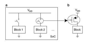
Figure 7: A power gating scheme in an SOC design
According to the functionality and activity of circuit blocks in the SoC, a block or several blocks can be individually powered off through the power switches. The static power dissipation on these powered-off blocks will therefore be minimized, reducing the overall power consumption of the SoC.
There are four type of power switches applied to create power gating. 1st Header switch controlled by P_sig as shown in figure 8a. 2nd Footer power switch controlled by N_sig as shown in figure 8b. 3rd Symmetric power switch architecture as shown in figure 8c. And 4th type of power switch is segmented power switch as shown in figure 8d. All power switches are having their own properties and implemented according to the physical parameters.
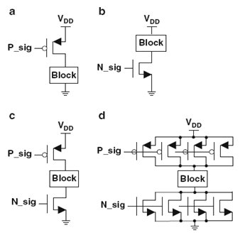
Figure 8: Example of power switch types
To test Header and Footer switch: (Goel et al. 2006) proposed using a comparator method to test the power switches. The basic idea of the method is to use an XOR gate as the comparator to compare the logic level value of the core’s power supply Vcore with the logic value of the standby signal, as shown in figure 9a.
The signal standby_f is the functional signal to control the operation of the power switch, while the signal standby_t is the test signal for the same operation. The signal standby_t can be provided by means of a shift register. The test-enable signal TE must be set to 1 so that the multiplexer placed in front of the power switch selects the signal standby_t.
However, there is one problem must be considered during this test. Here the Out signal is always “1” for correct power switch functionality. In this case, if there is stuck-at one fault at the output of XOR gate, it will mask the power switch faults and make them undetectable. To circumvent this issue, it is preferable to differentiate the control signal of the power switch and the input of the XOR comparator as shown in figure 9b.
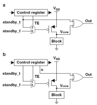
Figure 9: Test circuit to test header and footer type power switches
Controlling the n input of the XOR gate enables testing of both the power switch and the XOR gate. This allows fully testing the functionality of the power gating transistors and the test circuitry.
Test for segmented and symmetric power switch: The previous methods can also be extended for the symmetric and segmented switch test. For example, consider the comparator-based method proposed (Goel et al. 2006) to test the header and footer switches sequentially as shown in figure 10. Note that in a symmetric structure, there will be different control register and test enable (TE ) signals for testing the header switch and the footer switch.
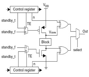
Figure 10: Test circuitry for symmetrical power switch
The segmented power switch can be tested segment by segment. Figure 11a shows the test circuitry for a two segment power switch. This design contains two segments and each segment contains two transistors. The two segments are controlled by control signal S1 and S2, respectively. The test pattern set and expected outputs are shown in figure 11b. In cycle 1, all the segments are turned off to see whether there is a permanent switch-on fault in segment 1 or segment 2. Next, in cycle 2, segment 1 is turned on to see whether there is a permanent switch-off fault in segment 1. In cycle 3, all the segments are turned off to discharge the Vcore node, preparing to test segment 2 in cycle 4. In this cycle, the switch-off fault in segment 2 is tested.

Figure 11: Test Circuitry and test patterns for segmented power switch
6.3 Testing Low Power Cell:
Design with different power domain and multiple voltages include a number of special cells such as SRRs, isolation cells, and level shifters. Those cells logically behave like regular gates during normal structural tests, and are therefore tested by conventional fault models. However, their low-power features create additional test requirements.
The ability of state retention registers (SRRs) to retain their state when the power domain is powered off needs to be validated during test. Conventional structural tests, if applied while a given power domain is forced on, cannot validate state retention since the domain is not powered off during the capture cycle. At a minimum, a test pattern such as the following must be applied to test the retention capability:
- Shift in value v .
- Enable retention, or pulse retention save clock.
- Enable isolation cells if this power domain feeds another that will remain on in the next step.
- Power the domain off.
- Power the domain on.
- Disable isolation cells.
- Disable retention, or pulse retention restore clock.
- Shift out, expect value v.
To cycle power during the capture cycles, the ATPG tool must be able to control the power mode.
Isolation cell is used to provide a reliable voltage level and corresponding binary value into a powered-on power domain when the source power domain is off, isolation cells must be tested under those conditions as well and not only when both power domains are on.
Isolation cells that are combinational gates such as AND or OR will only have one value on their output during isolation, that being the value when one of their inputs (the isolation enable signal) is forced to the gate’s controlling value. So when isolation is enabled, the output of an AND gate would be 0 and that of an OR gate would be 1. In addition to the tests normally applied to those gates when the power domains are on, it is sufficient to add one fault on the output of the isolation cell with a constraint that the input power domain must be powered off. If the isolation cell is a latch and can hold a 0 or 1 during isolation, then the cell needs to be tested for both output stuck-at faults. In both cases, of course, the source power domain must also be powered off when output of the isolation cell is observed by capturing the stuck-at fault effect.
Level shifter cells are inserted between power domains that operate at different voltage levels, and serve to convert the voltage levels up or down as needed by the driven domain. Functionally, the level shifter is often a buffer. In other cases, the isolation cell also performs the level shifting function. Level shifters are the simplest low-power cells to test. If the two power domains operate at fixed voltages, the level shifter is adequately tested by the conventional static and at-speed tests. If voltage scaling is used such that the two domains can operate at different voltage levels, the faults on the level shifter must be tested at the different operating conditions. The power modes specified by UPF or CPF can be analyzed to determine the different voltage levels at which those two domains can operate and therefore the different operating conditions at which the tests need to be repeated.
7. Conclusion
Testing complexity increases as low-power devices is making designs much more complex and very strictly optimized for power. Design for low power is changing the way designs are built and its testing rapidly became very intrusive at the point where all of the EDA tools need to be made power aware and must have unified support for users’ power intent for both designing and testing.
The goal of this paper is to study and implement low power designs and create environment around design suitable for testing the logic. DFT is implemented with different methods for testing both, core logic and power management circuits.
Reference
[1] Xijiang Lin: “Low power Testing – What can commercial Design For Test Tools provide?”: Proc. Journal of low power electronics and applications 9 December 2011
[2] Freddy Bembaron, Sachin kalkkar et al.: “low power verification methodology using UPF”
[3] IEEE P1801 Unified Low Power Format (UPF), 2007.
[4] Mark Kassab, & Mohammad Tehranipoor: “Test of power management structures”. Proc. Power aware testing and test strategies for low power device.
[5] Saqib Khursheed, & Bashir M. Al-Hashimi: “Test strategies for multivoltage design” Proc. Power aware testing and test strategies for low power device.
[6] Mokhtar Hirech: “EDA solution for power aware design for test”. Proc. Power aware testing and test strategies for low power device.
[7] Chickermane, V.; Gallagher, P.; Sage, J.; Yuan, P.; Chakravadhanula, K. A Power-Aware Test Methodology for Multi-Supply Multi-Voltage Design. In Proceedings of the International Test Conference, Santa Clara, CA, USA, 28–30 October 2008; Paper 9.1.
[8] “Synopsys Low-Power Solution” White paper, June2007.
Related Semiconductor IP
- Ultra-Low-Power LPDDR3/LPDDR2/DDR3L Combo Subsystem
- 1G BASE-T Ethernet Verification IP
- Network-on-Chip (NoC)
- Microsecond Channel (MSC/MSC-Plus) Controller
- 12-bit, 400 MSPS SAR ADC - TSMC 12nm FFC
Related Articles
- Low Power Design in SoC Using Arm IP
- Akida Exploits Sparsity For Low Power in Neural Networks
- PCIe 5.0: The universal high-speed interconnect for High Bandwidth and Low Latency Applications Design Challenges & Solutions
- Low power is everywhere
Latest Articles
- Extending and Accelerating Inner Product Masking with Fault Detection via Instruction Set Extension
- ioPUF+: A PUF Based on I/O Pull-Up/Down Resistors for Secret Key Generation in IoT Nodes
- In-Situ Encryption of Single-Transistor Nonvolatile Memories without Density Loss
- David vs. Goliath: Can Small Models Win Big with Agentic AI in Hardware Design?
- RoMe: Row Granularity Access Memory System for Large Language Models