An ESD efficient, Generic Low Power Wake up methodology in an SOC
By Naveen Kuma, Rakesh Pandey, Rishi Bhooshan (Freescale Semiconductors)
As the semiconductor industry is moving towards lower technology nodes, more and more complexity is being introduced in the design to beat the competition and provide most innovative solution to cater the needs. One of the biggest challenges that the designer faces is in terms of the keeping the power budgets of the chip within the specification and even innovate to reduce the current numbers. Depending on the application requirements, the designers have to tune up the power profile of the SoC. There are various ways to do so like dynamically changing frequency and voltage of operation, considering system level contributions to power consumption, using various modes of operation etc. In most of the cases, SoC has to support various power modes like Run mode, Sleep mode, Halt mode etc. Different power numbers are defined for each mode. Run modes can further be divided in various sub modes depending on application.
In very low power mode, only small relevant logic (and may be small system memory) is kept alive (powered up) and rest of the chip is powered down. This logic retains bare minimum functionality and is complemented by a wake up logic which allows the microcontroller to exit this low power mode and become fully functional. There is a certain amount of time required by the system to reach full run mode from standby mode. The wakeup is mainly based on external indication through pads and/or internal triggers (from within the ON domain).
While implementing a wake up scheme, the designer faces complex challenges throughout the design cycle including implementation of various power domains in SoG(sea of gates) and implementation in padring section. In this article, we will focus on implementation of wake up functionality in the padring section, discuss the various schemes and their limitations and present a low power wakeup scheme that is simple, generic, with minimal changes (overhead) to the existing I/O pad library.
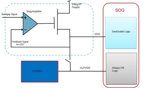
Figure (1) illustrates a generic power management unit providing a switchable and always ON power supply to the SoC.

Figure 1: Generic Power Management Unit in a SoC
The wakeup is mainly based on external indication through pads and/or internal triggers (from within the ON domain). The internal trigger comes from the standby Logic. Wake up trigger can be provided through I/O pads using various communication interfaces like CAN, SCI or ADC or other digital/analog interfaces. I/O pads are interface of the die to the external world. Generally the I/O pads work at a higher voltage (may be 3.3V or 5V) and core logic is working on lower voltage (1-1.4V).
In most of the designs, the general implementation is to have a power on reset (POR) signal being generated from power management unit and this signal goes as an input to a special I/O pad called “voltage detection pad” which detects if the core voltage is powered up when the I/O voltage supply is enabled. The output of this voltage detection pad goes to all I/O cells via a ring in padring (or may be core region based on I/O architecture). Based on the comparison, if core voltage is not powered up while I/O power is enabled, this signal would tristate all the drivers connected to I/O power.
Common Wake up schemes implemented in I/O pads and their limitations:
Existing wake-up scheme used special I/O cell types to bring in external wakeup signal for the IC to exit from low power mode. This increases integration time with new ESD rules for new pads. This also increases numbers of I/O cells in the library to support. There are voltage detection cells that need to be supported for the switchable supply as well as custom made voltage detection cells required for ‘always ON’ supply. Since majority of the logic and I/O pads work with switchable supply, there are rings of this supply inside pads. For the custom cells to detect the ‘always ON’ supply, there are modifications required in the I/O cell architecture and provide core side ports for supply as well as output signal. This introduces extra burden on the library developers to support these cell sets with all views. For the designer perspective, ESD rules for these new pads need to be taken care and these require extra pads placement requirement, resulting in die size increase.
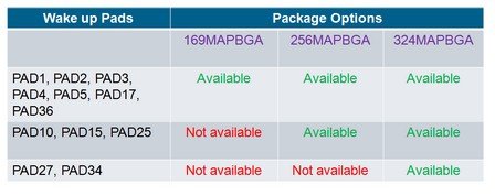
Most of the chips target for multiple package solution for different functionalities as per the requirement by various customers. There can be a case that there can be all wake up pads that are available in one package but some of these wake up pads are not bonded in other packages. For example, let us assume a die supports three package configurations like 256MAPBGA, 169MAPBGA and 324MAPBGA and the wake up functionality is defined as shown in table 1.

Table1: Wake-up pads available in different packages.
The analog resistive path of the pad is used for wake up signal and it requires being level shifted before reaching wake-up logic. In such cases, there is additional AND operation logic of package decode bits and wake-up signal to be implemented in SoC. The package decode bits needs to be stored in memory and that memory cell need to be powered up all the time for proper functionality. This approach increases the leakage power of the design and introduces high dependency on package decode bits.
Other scheme used a separate I/O segment with additional ESD termination to protect this small segment. This increases I/O ring size and leakage and additional segment is needed if more than one wakeup site is required, which substantially reduces the flexibility in pad placement.
Due to one or the other reasons out of what we discussed, the designer has to look out for a generic solution.
Generic, Self ESD protected wake up scheme with minimal I/O overhead:
This new wake-up scheme allows regular I/O cells to be used, simplifying I/O ring integration. This reduces integration time and time to develop new I/O cells. The new scheme is flexible that can be used with any I/O cell in the library, and can be placed in the middle of any I/O segment in the I/O ring. This scheme provides self reliant ESD protection with no additional structure for ESD protection.
There needs to be introduced a small cut cell, which cuts the core voltage supply (VDD) and isolates the wake-up pads from rest of the I/O segment , and at the same time provides core voltage detector circuit using separate ‘power on reset’ signal from Power Management Unit (PMC). This new cut cell provides the flexibility in pad placement. This new core voltage cut cell with core voltage detect circuit is placed on both sides of the intended wake-up pads to cut core VDD and to provide ‘power-off’ signal from ‘power-on-reset’ signal from PMC to disable wake-up pads to eliminate the need to safe state of I/O control signal in low power mode. The whole system goes in standby mode when there is no more requirements for system to run, however, the pads with standby power are alive and continue to receive controls from the core side alive logic, which keep the pad at a certain pull level. This means that no additional logic is required for gating the un-bonded pads. The pad controls keep the pad at required state and prevents floating nodes. For Wakeup, any activity on wake-up pads will make the system wake-up and enable the wakeup sequence. The wake-up unit and wake-up pads use always-on domain supply so that these circuits are always ON for receiving any activity from system to wake up the core system.

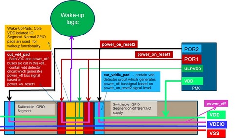
Figure2: Generic Wake Up Scheme Implementation in Padring
Figure 2 shows the implementation at SoC level. As discussed above, the new cut cell called “cut_vdd_pad” is placed on both sides of wake-up pads. This cell cuts the core voltage (VDD) rail in I/O pads. ULPVDD is always ON supply provided by the PMC. Now these wake up pad from sort of a virtual separate bank. We call it “virtual” since these are actually placed in a GPIO bank working on the I/O supply of GPIO bank and hence are not actually a padring bank.(Padring bank is a terminology used to define a particular set of I/O pads working on same I/O bank supply.) Since this is not an actual bank, therefore no separate ESD protection measures are required. This new cut cell provides the “power_off” signal based on a separate “power_on_reset1” signal provided by PMC. There is a separate power-on-reset signal generated by PMC for other I/O cells having switchable core supply. The only overhead in such approach is the extra space (which is as small as few microns) required in padring for placement of this new cut cell. The important point is this cell has VDD detector circuit.
Summarizing the advantages of this generic scheme as below:
- This wakeup scheme allows the wakeup pads to be interspersed in the pad ring anywhere. All overhead it has a cut cell on either side of the pad. Multiple wakeup pads can be clubbed together with cut cells at the far ends.
- This solution does not require package specific wake-up solutions. Prior approaches required different implementation for different packages as some of the wake-up pads were not there in few packages. This saves a potential leakage situation during power up.
- The core-VDD-isolated wake-up pads can be placed in the middle of any I/O ring segment, thus keeping the padring flexibility intact. It does not need any special consideration. The cut cell architecture does not deteriorate characteristics or reduces the flexibility of pin placement of these interfaces.
- Existing approaches keep whole padring wake-up segment in the always on domain supply but that would increase leakage current on ULVDD in standby mode. This new isolated-pad wakeup scheme significantly reduces leakage current drain ULVDD supply.
- This scheme automatically takes care of other ESD requirements and IO integration requirements without any extra efforts. ESD protection uses the I/O segment protection. Previous art using the analog path of the pad had to use additional ESD logic.
Conclusion:
We think that the technique described here can be used in all SoC with multiple packages and different low power modes though it will involve a small cut cell design and placement as described. Still when it comes to the flexibility and risk free implementation, this solution is worth looking for.
Authors Biography:
Naveen Kumar is working as a senior design engineer at Freescale Semiconductor, India Pvt Ltd with more than four years of experience in SOC physical design activities.
Rakesh Pandey (rakesh.pandey@freescale.com) is a Design Manager for Automotive IC’s with Freescale.
Rishi Bhooshan is Senior Member of Technical Staff (SMTS) at Freescale Semiconductors, India Pvt Ltd having experience in the area of Physical design, chip design tools, flows and methodology including design methodology such as low power design, power integrity and signal integrity, ESD/EMC and reliability.
Related Semiconductor IP
- Ultra-Low-Power LPDDR3/LPDDR2/DDR3L Combo Subsystem
- 1G BASE-T Ethernet Verification IP
- Network-on-Chip (NoC)
- Microsecond Channel (MSC/MSC-Plus) Controller
- 12-bit, 400 MSPS SAR ADC - TSMC 12nm FFC
Related Articles
- An Efficient Device for Forward Collision Warning Using Low Cost Stereo Camera & Embedded SoC
- An Efficient ASIP Design Methodology
- An RTL to GDSII approach for low power design: A design for power methodology
- An efficient way of loading data packets and checking data integrity of memories in SoC verification environment
Latest Articles
- Extending and Accelerating Inner Product Masking with Fault Detection via Instruction Set Extension
- ioPUF+: A PUF Based on I/O Pull-Up/Down Resistors for Secret Key Generation in IoT Nodes
- In-Situ Encryption of Single-Transistor Nonvolatile Memories without Density Loss
- David vs. Goliath: Can Small Models Win Big with Agentic AI in Hardware Design?
- RoMe: Row Granularity Access Memory System for Large Language Models