Low Power Analysis and Verification of Super Speed Inter-Chip (SSIC) IP
Srikanth Vadanaparthi, Shekhil Hassan Thavalengal (Synopsys (India) Pvt. Ltd)
I. Abstract
Low power technology is now a vital part of VLSI design as the need to reduce power consumption has become a global concern. The power consumed by various portable and non-portable devices has increased because of an explosion in the sophisticated features supported. The battery capacity has not increased in the same scale thereby resulting in limited operating time of the portable device. The environmental issues because of increased power consumption and heat dissipation have become a concern. Low power technology thus has emerged to become a vital part in VLSI design that enables consumers to operate devices for a longer time with better performance with no significant increase in power consumption.
IP standards such as USB [1], PCI Express, HDMI and Ethernet are predominantly used in laptops, desktops, notebooks, mobile devices and PDAs. Mobile devices have also raised the need for higher battery life. This means that designs need to be implemented with power aware architecture with low power techniques. The recent standardization trend is to have power aware intelligence built into the standard itself leaving the implementation open to the respective designer.
The USB standard has evolved over decades and has emerged to be one of the major current generations of peripheral-interconnect. Super Speed supports a 5 Gbps signaling rate offering 10x performance increases over Hi-Speed with optimized power efficiency and full duplex communication. Introduction of lower, active and idle power management has itself proven to be power efficient. In addition, consistent with recent power efficiency trends, the USB 3.0[2] standard defines U1, U2 and U3 low power states. Each state differs in percentage of power consumption reduction as well as latency for waking up from low power state.
Super Speed Inter-chip (SSIC)[3] technology built on top of Super Speed USB 3.0 for chip to chip interconnect applications exploits the USB 3.0 protocol with MIPI Alliance physical interface (M-PHY)[4] to achieve performance in mobile platforms and laptops. In addition to supporting the USB 3.0 U1, U2 and U3 states, SSIC supports placing the M-PHY in stall state as soon as the bus idle is detected. Implementing SSIC reduces chip-to-chip power consumption by up to 80 percent compared to conventional USB 3.0 technology for mobile and wireless devices.
SSIC can be used in wireless chips like Wi-Fi chipsets and LTE modems. This allows you to save power in your mobile phone by using SSIC inside the phone, on PCB to the main mobile application processor. SSIC chip-to-chip interconnect can re-use existing USB 3.0 software and drivers to save years of engineering effort.The USB subsystem which already exists in mobile devices has made SSIC adaptable to existing subsystem. M-PHY has a serial physical layer technology with high bandwidth, required for mobile applications with high power efficiency with different low power states during idle and active conditions. M-PHY achieves higher power efficiency by implementing low power mode and active mode. The switching between these modes at appropriate time and condition to maximize power saving by minimal impact in performance favors current IP subsystem.
The SSIC specification defines the low power states and allows implementers to choose how much power must be saved in each state. Until recently, most semiconductor devices supporting low power mode used to do it using clock gating. In this mode, during idle and suspend conditions, clocks are shut off to reduce dynamic power consumed by the design. However, clock gating does not prevent leakage of power.This has become an increasing challenge with battery operated mobile and portable devices.
SSIC communication targeted for mobile platforms uses deep sub-micron technologies. Both dynamic power and leakage power are significant in deep sub-micron technologies. Thus, the need to optimize the distribution of power completely to portions of the device during idle modes became critical. This has resulted in new techniques such as multi voltage design practice, Power gating, Back bias, and Multi-rail retention [5].
In our current work, we focus on the low power analysis and verification challenges and the methodology used to verify low power design. The power-gating feature that we term Hibernation brings in significant power savings to Synopsys SSIC IP Controller. The verification tests the functionality of the Controller before, during and after hibernation state. The low power analysis will showcase the power savings achieved in SSIC IP with and Without Hibernation.
This paper discusses the following topics:
- Section II provides an overview of SSIC Technology.
- Section III discusses the Hibernation functionality for USB 3.0 SSIC IP.
- Section IV discusses the details of power aware verification and methodology.
- Section V discusses the power saving details for SSIC IP with and without Hibernation feature enabled during suspend cycle.
- Section VI provides relevant conclusions.
II. Overview of SSIC Technology
USB ports are very common in daily life. For example, a USB 2.0 webcam uses a USB 2.0 PHY connection (with a cable) to a USB 2.0 PHY on the motherboard (internally). The webcam manufacturer can easily implement standard USB 2.0 drivers for both the embedded webcam on the PCB SoC and the external webcam. The disadvantage to the PC designer is that these two USB 2.0 PHYs drain the battery because they double the required power.
To save power for such applications, the USB standard committee has introduced Hi-Speed Inter-chip (HSIC)[6] solution which removes the analog portion of the USB 2.0 Physical layer. Previously, a USB 2.0 signal was converted from digital to analog, transmitted over a wire, and converted back from analog to digital in the USB PHY on the other SoC. With the new HSIC standard created by the HSIC USB-IF Working Group, signals can stay digital, be transmitted to the PCB over standard FR4 traces, and be received at the destination.
The USB 2.0 HSIC PHY is one-third the size of a standard USB 2.0 PHY and consumes less than one-third the power. Active power in an HSIC PHY cuts power in a pair of devices by 72% [7], so major application processors for smartphones and LTE/3G modems now use HSIC.
HSIC has been successful, but can be lacking as shown in the following example: A typical single USB 2.0 host can support only an effective throughput of 320 to 390 Mbps.if you have a USB 2.0 hard drive (externally) and an HSIC modem (internally) connected to the same USB 2.0 host, and the hard drive consumed the throughput, then either the HSIC modem becomes starved for data or the bandwidth is split and file transfer speed is reduced by 30-50%. USB 2.0 cannot meet the throughput requirements of these applications.
The M-PHY standard consumes lower power and offers greater flexibility than USB 3.0 PHYs. SSIC supports the following Gears of M-PHY:
- Gear1 -- 1.25 or 1.45 Gbps
- Gear2 -- 2.5 to 2.9 Gbps
- Gear3 -- 5.8 Gbps
In addition, M-PHYs can have 1, 2, or 4 lanes. Each lane has x pins, so 2 lanes have 2x pins and 4 lanes have 4x pins. These lane configurations offer flexibility to run in multiple parallel lanes at slower clock speeds to save power, or to run at faster speeds but consume fewer pins. Because many SoCs are pin and/or pad limited, designers looking for high throughput often choose the faster Gear3 standard to save pins. A 1 lane M-PHY has 16 pins. A standard USB 3.0 PHY has at least 15 pins including USB 2.0 D+ and D-; USB 3.0 Tx+,Tx- Rx+, Rx-, power, and ground pins.
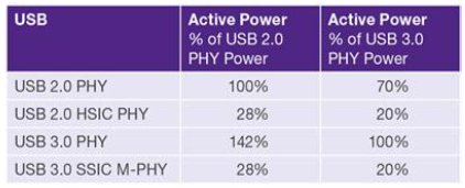
Table 1: USB PHY Power Comparisons
Table 1 shows the power comparison of different USB PHY. Just as the HSIC PHY is smaller than a USB 2.0 PHY, the MIPI M-PHY is about 50% smaller than a USB 3.0 PHY. The introduction of the HSIC specification enabled an on-PCB interface with 67% power savings over USB 2.0 PHY. SSIC brings 80% power savings using a MIPI M-PHY and SSIC, as compared to a USB 3.0 PHY. The SSIC standard improves power efficiency while reducing area and maintaining throughput and preserving SSIC software compatibility.
III. Overview of Hibernation functionality of USB 3.0 SSIC IP
With different power reduction techniques widely used for dynamic power reduction, the leakage power consumed by design has become a major concern for sub-micron technologies. Hibernation reduces leakage power consumed by controller and hence reduces the overall power consumption. Switching off the power supply to design blocks which are in suspend state or low power mode reduces the leakage as well as dynamic power.
A typical USB 3.0 SSIC IP provides Hibernation functionality where the design shuts off power to the controller when certain conditions for suspend are met and keeps wake up logic to run at lower clocks to detect any remote wake up. On suspend, Hibernation entry is initiated and only critical information is stored in the wake up logic. After Hibernation entry, power supply to the Controller is shut off and certain state and register values are stored in the buffer outside the SSIC Controller. Hibernation wake up can be done from software as well as from the remote partner, which is detected using a wake up logic. During Hibernation exit, critical information required for the Controller to start normal operation is restored followed by state and register values from external buffer. The Controller must start normal operation after the Hibernation exit sequence is complete.
During the actual power cut off state, the power consumption is only from wake up logic and the MPHY. The M-PHY can also be put into low power state or reset, as the controller itself is powered down, thus reducing the overall power consumed by the product.
Figure 1 shows the block diagram of Hibernation functionality in SSIC IP that has two power supplies, Vcc and Vaux. Vcc is the power supply to the USB SSIC IP and Vaux is the power supply to always-on block and the power controller.
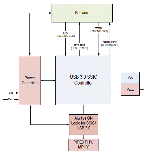
Figure 1: Hibernation block diagram in SSIC IP
Critical information is saved when Hibernation is entered and the module saves its state to always-on block and restore once Vcc is back. Software initiates the save and restore of register information saved outside controller and the power controller initiates the save and restore of critical information from always-on block.
Typically Controller should be either suspend (U3) or disconnected state to start Hibernation entry process. The controller triggers SSIC Hibernation entry Interrupt which must be used by software to start hibernation entry flow. Then the SW and HW interact (through USBCMD.CSS and USBSTS.SSS [8]) to ensure that the generic register information is saved by the controller. The software can then request for D3 state entry and Controller saves the critical information in always-on block. Once the save is completed, the power controller can set the Controller to D3 and on confirmation of D3 entry from controller, Vcc is removed to the controller.
Low power exit can be either through software or MPHY initiated. When the software requests for D3 exit, critical information and states must be restored by controller and always-on block must confirm the D0 entry. To restore register information, USBCMD.CRS is set and software must wait for USBSTS.RSS to be reset which ensures restore is completed by controller. Software must also initialize needed xHCI registers and restart the previously running EP's.
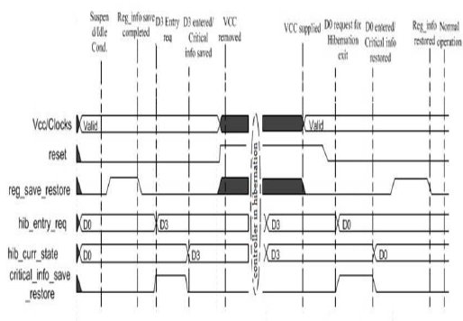
Figure 2: Hibernation Entry-Exit Initiated by Software
Figure 2 shows the hibernation entry - exit initiated by Software where Vcc power supply is removed after entering D3 and shows different steps involved during Hibernation entry and exit.
If the exit is initiated by M-PHY, the controller asserts wake up signal to restore power to controller and wakeup host software. The wake up logic in always-on block detects the wake up condition from M-PHY interface and assert wake up signal, which is communicated to the power controller and this is informed to software with an interrupt and the same steps for software initiated wake up is performed.
IV. Low power Verification
The Always-on block and Power Controller blocks are very small but have far-reaching impact on the Controller's activities. Power aware simulations must be integrated as part of the functional verification of the Controller and all the entry and exit mechanisms of U3 power state.
The verification must also ensure that the Controller is able to transition from one mode of operation to another - mode: fully functional, maximum power down modes (Hibernation); that the design responds to stimuli appropriately to go through the correct state transition Sequences. Thus, coverage to include power savings mode and the need for assertions and other testbench infrastructure to cover power management becomes important. The fact that ordinary simulators used for verification do not typically model Vcc cut-off, gives rise to the need for Voltage aware simulators [9].
The power aware verification flow must cover the following verification space:
- Incorrect application of voltages/unplanned voltage states,
- Power on reset sequences,
- Voltage monitoring and handshake logic errors,
- Logic conversion errors,
- Memory corruption and voltage race errors.
Figure 3 depicts the block diagram of the testbench used for the verification of the SSIC IP controller.
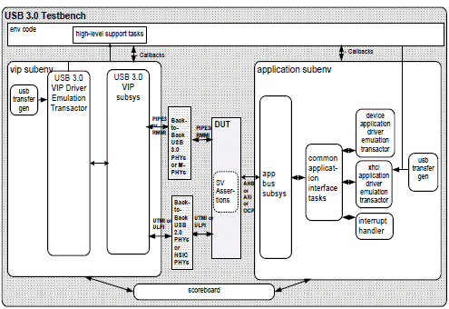
Figure 3: USB 3.0 SSIC Random TE
The Unified Power Format (UPF) defines both language format and semantics to convey the power intent information of a design to the simulation, synthesis and backend tools.
UPF for USB 3.0 SSIC IP is brought up by defining two power rails, VDD-ON and VDD-PWRDN, and power domains, ALWAYS_ON and PWR_DN, which are used to analyze the functionality of the Controller when it is put into Hibernation, D3. Isolation cells are provided for always-on logic output to restrict X-propagations to prevent power drainage from ALWAYS_ON. Power switch was placed for controlling power supply to the PWR_DN. During Hibernation, as the Controller is put into D3 with proper application programming, the power supply to controller is completely switched off. This reduces the leakage power consumed by the Controller and it switches wake up logic clocks into lower frequency to minimize the dynamic power consumed. According to the flow, reset must be applied before shutting of power supply to ensure that the Controller is in a valid state during wake-up. Power states are switched according to the D3 request by the power controller, which is triggered from the application layer. The application layer must follow the necessary Hibernation entry flow before requesting D3. After entering D3, as the Controller power is cut off, the VDD-ON supply is used by the wake up logic to detect remote partner request. Hence Dual power rail is used in UPF flow with VDD-PWRDN and VDD-ON as power supply to respective power domains. Fig 3 shows the VMM based Constrained Random Verification (CRV) Test Environment (TE) setup for Verification of SSIC IP which is reused for this flow.
Figure 4 shows the UPF Simulation Snapshot with important signal transitions during hibernation entry and exit states with series of events relevant to hibernation flow.
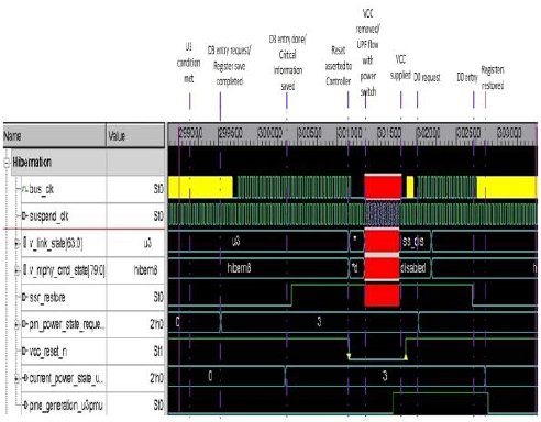
Figure 4: Hibernation Entry ¡VExit Simulation snapshot with UPF flow
The following verification space needs to be covered for Hibernation power management feature:
- Hibernation Entry stage
- Controller in Hibernation
- Hibernation Exit stage
Hibernation Entry stage is verified when SSIC Link moves into U3 and Controller triggers Hibernation entry interrupt. This should be used by application to put the Controller into low power by D3 request and followed by shutting down the power using power switch provided in UPF. Controller is now in Hibernation and now we see in Figure 4 the internal signals are in unknown state (X) as expected.
In Hibernation state, the isolation cells must be active thereby the output of power down is clamped to a specific value as specified in UPF. In this state, the power consumption is only from the ALWAYS_ON block, which runs in lower clock frequency. Remote partner wake up is detected by ALWAYS_ON block, which detects Hibernate exit from remote partner and signals wake up to power controller which trigger Hibernation Exit. Hibernation exit must start with supply to power down block, followed by restore of critical information and the Controller then start work normally.
In our current work we have used the native low power methodology in Synopsys VCS for Multi voltage simulation and Design Compiler and Prime time PT for power analysis.
V. Low power analysis of USB 3.0 SSIC IP
SSIC features, along with the MIPI M-PHY, provide significant reduction in active power. In this section, we aim to show significant reduction in active and leakage power from controller during Hibernation Cycle.
USB port is mainly used for burst data transfer where the bus is not always functional. There are many idle cycles between data transfers in USB system. These idle cycles give many opportunities to implement a power aware design and save power.
USB 3.0 functionality is broadly segregated into the following power states:
- U0: The USB bus is fully functional and there is a data transfer on bus.
- U1: Bus is Idle for few tens of microseconds and there is no data transfer on the bus.
- U2: Bus is Idle for few hundreds of microseconds and there is no data transfer on the bus.
- U3: Bus is Idle for few milliseconds and there are no data transfers on the bus.
After defining the power states, we can define how hibernation can be used to achieve maximum power reduction. Our current work focus is on U3 power state. U3 is an ideal choice for implementing power-gating features for reducing leakage power. The standard allows ample time for the Controller to enter and exit U3 state. Power gating requires at least two power rails so that the VDD to the unused logic can be switched off. The remaining logic detects activity on the bus and wakes up the switched off logic when required.
Following section describes simulation based measurements done using UPF flow along with Multivoltage simulation tool. The power analysis is done during U3 state with same simulation carried out for design without hibernation feature and with hibernation feature. The relative power comparison is made after using UPF flow for Hibernation feature in Synopsys Prime Time PX where the waveform dump is used as activity for time based power analysis along with netlist generated from Synopsys Design Compiler.
Figure 5 shows the comparative power savings of the total power reduction only during the Hibernation Cycle to highlight the amount of power saved.
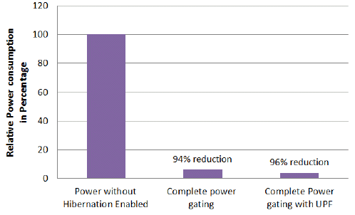
Figure 5: Relative power consumption during hibernation cycle
Figure 6 shows the comparative power savings of the leakage power reduction only during the Hibernation Cycle to highlight the amount of power saved.
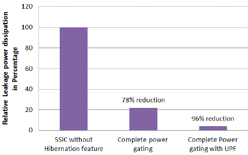
Figure 6: Relative leakage power dissipated during hibernation cycle
VI. Conclusion
Introduction of High-speed inter-chip USB has allowed chip designers to use the USB in Mobile chipsets with limitation on speed. Introduction of SSIC has overcome the limitations of HSIC and reduced the active power consumption by 80% using M-PHY compared to regular USB 3.0 if used for Inter-chip connection.
The current work describes the challenges and workable methodology to verify the Complex IP systems from the application programming sequence to the correct functionality of the Power management unit using Native Low power mode in VCS simulator and VMM methodology. The current work also highlights the additional power savings that can be achieved by keeping the SSIC IP in Hibernation mode during long idle cycles.
REFERENCES
[1] USB Standard, Universal Serial Bus Specification, Rev 2.0, April 27-2000
[2] USB Standard, Universal Serial Bus 3.0 Specification, Rev 1.0, June 6 , 2011.
[3] Inter-chip supplement to USB revision 3.0 specification, Rev 1.1, Feb ¡V 2013.
[4] MIPI M-PHY Specification version 2.0 , revision 2.0 , April 2012
[5] S.Jadcherla, J. Bergeron et al., ¡§Verification Methodology Manual for Low power,¡¨ Synopsys Inc., Feb. 2009, ISBN 978-1-60743-413-9.
[6] High speed Inter-chip USB Electrical Specification, Rev 1.0, September 23 ¡V 2007.
[7] DesignWare Synopsys Technical Bulletin on USB SSIC
[8] eXtensible Host Controller Interface for Universal Serial Bus (xHCI) specification Rev 1.0 ¡V 5/21/10.
[9] Keating M., et al, Low Power Methodology Manual for System-on-Chip design, Springer 2007, ISBN 978-0-387-71818-7
Related Semiconductor IP
- NPU IP Core for Mobile
- NPU IP Core for Edge
- Specialized Video Processing NPU IP
- HYPERBUS™ Memory Controller
- AV1 Video Encoder IP
Related White Papers
- Challenges and Benefits of Low Power Design Verification with CPF for a standalone IP
- How Low Can You Go? Pushing the Limits of Transistors - Deep Low Voltage Enablement of Embedded Memories and Logic Libraries to Achieve Extreme Low Power
- High Speed, Low Power and Flexibility Drive DisplayPort's Increasing Popularity
- Robust Low power Architecture verification Strategy
Latest White Papers
- Transition Fixes in 3nm Multi-Voltage SoC Design
- CXL Topology-Aware and Expander-Driven Prefetching: Unlocking SSD Performance
- Breaking the Memory Bandwidth Boundary. GDDR7 IP Design Challenges & Solutions
- Automating NoC Design to Tackle Rising SoC Complexity
- Memory Prefetching Evaluation of Scientific Applications on a Modern HPC Arm-Based Processor