Layer 2 Switch Implementation with Programmable Logic Devices
An der Steinernen Brueke 1 -- D85757 Karlsfeld, Germany
Abstract
The paper describes how, with a SOPC (System on a Programmable Chip) architecture embedded with a 32-Bit NIOS-II, a Layer 2 Ethernet switch can be implemented in a FPGA (Field Programmable Gate Array) devices to provide increased flexibility compared to standard L2 Switching ASSP (Application Specific Standard Part).
L2 Switching Overview
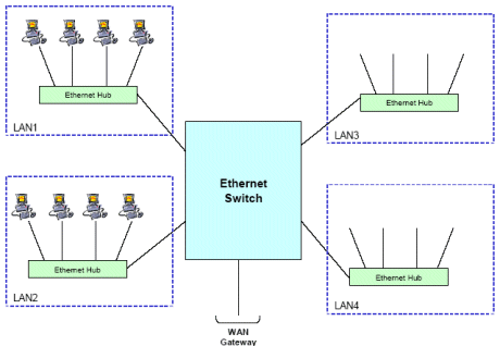
An Ethernet switch is used to interconnect a number of Ethernet LANs (Local Area Networks), forming a large Ethernet network. Different ports of the switch are connected to different LAN segments. The purpose of the switch is to forward the packets intelligently, only to the desired destination segment of the network whenever possible, instead of flooding the network for every frame. The switch stores the MAC addresses observed from frames received through each port and uses this information to learn which MAC belongs to which segment of the network. With this information, the switch can forward the frames from the source network segment to only the destination, instead of forwarding the frame to all the connected ports, reducing the network load.

Figure 1: Switched Network Overview
SOPC Advantage vs ASSP
Standard Ethernet multi-port Ethernet Switches ASSPs are widely available from different vendors and can be used to meet the requirements of a large number of applications. However as standard parts are typically designed for “Typical” networking applications and may not provide a good solution for applications that required specific features.
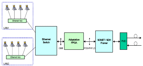
For example, standard Ethernet Switches typically only implement physical Ethernet interfaces such as MII Medium Independent Interface (Fast Ethernet ports) or GMII Gigabit MII (Gigabit Ethernet port) and therefore require an adaptation device if one or multiple ports need to be connected to, for example, a PCI bus, a SONET / SDH framer for POS (Packet Over SONET / SDH) for EOS (Ethernet Over SONET / SDH) applications or voice processors for VoIP (Voice over IP) applications.
In addition, standard Ethernet switches typically implement a large number of ports (12, 24) and implement a fixed distribution of ports (e.g. eight 10/100 Ethernet ports + 1 Gigabit Ethernet port) and therefore can provide an oversized or not adapted solution for applications that require only a few ports or a different repartition of ports.
With standard devices it is also not possible to implement non standard Ethernet ports such as a 2Gbps port.

Figure 2: Discrete Application Overview
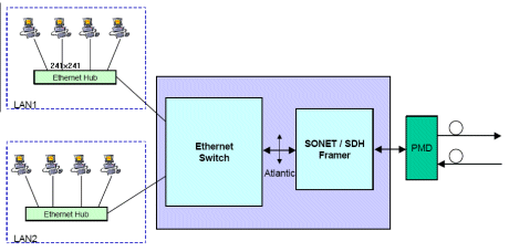
To overcome the limitations of standard devices, MorethanIP has developed a flexible Ethernet switching engine which provides a unique solution that allows designers to implement any additional function (e.g. PCI interface, POS-PHY / SPI packet interfaces,…) to complement the Ethernet switch and to provide connectivity to a large number of standard parts (e.g. SONET / SDH framers, VoIP processor) or systems (e.g. Proprietary backplane, host computer via PCI / PCI-X) with a single chip solution.

Figure 3: Integrated Application Overview
The switch can also be implemented in Altera Stratix or Stratix-II high integration programmable a solution that provide on board configuration capability that can be used to change the Switch functionalities on board.
L2 Switch Architecture
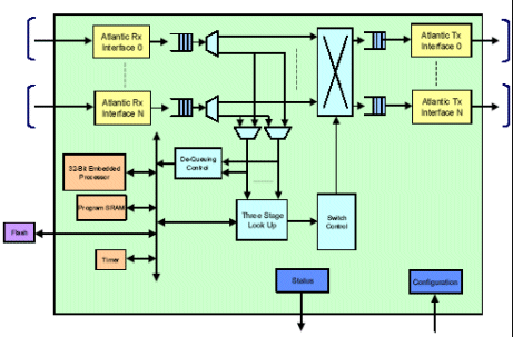
MorethanIP switch is implemented as a System on a Programmable Chip (SOPC) and it embeds a Hardware switch engine, to provide high performances, and a 32-Bit NIOS-II processor, which performs the table management tasks like learning, ageing, migration. Using an embedded processor also allow designers to implement any other high level networking functions such as Spanning Tree algorithm or any user specific task.
The switch implement a programmable number of ports, which are physically implemented with Atlantic ports (Simple Master / Slave FIFO based interface) on which any Layer 1 application or standard board level interface can be connected.
The MorethanIP programmable switch provides 6Gbps-switching capability, which can be used as required in a custom application. For example, the Switch can be configured to implement four Gigabit Ethernet ports and twelve Fast Ethernet ports or non-standard configurations such as a 2Gbps port with multiple 200Mbps ports.

Figure 4: Switch Block Diagram
The switch does not require any external device apart from a Flash to boot the embedded processor to reduce the solution cost and improve system level integration.
Functional Description
Overview
Frame switching is based on two-stage hash code look-up associated with a linear searching. This solution provides high performance and enough flexibility to extend the maximum number of MAC addresses supported by the standard implementation of the switch (2048 Addresses). To provide maximum performance and a non-blocking operation, frame switching is performed at wire speed without any software or firmware overhead.
To manage the switch look-up table a 32-Bit processor NIOSII is implemented in the switch. To control the switch, a firmware as been developed which performs the following tasks:
- MAC Address Learning
- Look Up table entry ageing
- Port migration
- Hash code and table management
The Hardware and Software parts of the Switch have been designed for performance and therefore tightly coupled. The switch architecture is easily scalable to support higher throughputs (e.g. 10 Gigabit switch Core).
Frame Switching
The 48-Bit destination MAC of each frame received by the Switch, on any of its interfaces, is extracted by the de-queuing Hardware and provided to the look-up engine together with the physical interface number.
If the received frame is a Unicast frame a Three-Stage switching process is implemented. The Three-Stage look-up engine first calculates the 8-Bit hash value from the MAC address 24-Bit serial number. The 8-Bit hash code is used as an entry to the Switch look-up table. The look-up function can provide three results with tree different associated actions performed by the switch Hardware:
- The address is in the table and associated with a correct port number:
The switch forwards the frame only to the looked up port.
- The address is in the table but is associated with the port on which it was received:
The switch discards the frame and does not forward it to any port.
- The address is not found in the table:
The Switch engine sends the received frame to all ports except the port on which it was received.
If a Broadcast or a Multicast frame is received, the switch Hardware sends the received frame to all output ports, except the one from which it was received.
Learning
The Switch frame de-queuing Hardware extract the destination MAC address of each frame received on each of the switch port and provide it, via a Hardware queue to the Switch Firmware which implements the learning task. The task is executed as follows:
- For every frame received, the source address is compared with the previously stored entries in the look up table. If it does not match with any of the previous ones, it is stored in the table. The following information are stored for each entry:
- MAC address: the 48-bit address is stored in the table.
- Time stamp: a 10-bit value, used to determine the age of an entry.
- Port number: a 4-bit value, which indicates the port through which the frame was received.
- Status: a 2-bit value. One bit indicates whether the entry is valid or invalid. The other is reserved.
- If there is no more space in the tables for new entry, the oldest entry is removed and replaced by the new record..
Migration If the Firmware received a MAC address which is already in the Switch tables but associated to a different physical port number (Indicating that a station was moved from one network to another). The Firmware performs the following tasks:
- The entry corresponding to the MAC address is updated with the new port number.
- The time stamp of the updated entry is set to the current time.
Ageing
It refers to the time stamping and deleting the old entries. It proceeds as follows:
- The time stamp is stored with all the entries and is updated each time the source address appears again.
- If a record is not updated for a period of time, it is removed from the table. This process runs continuously in the background. The aging period is programmable between 1 to 6 minutes.
Conclusion
Layer 2 switches being an essential building block in todays Telecommunication system a and with the availability of high performance and high integration programmable logic devices, like the Altera Stratix or Stratix-II FPGAs, new integration possibilities are now available. Complex programmable system chips can be designed to replace standard parts, achieve higher integration and design devices highly optimized for a particular application.
Related Semiconductor IP
- NPU IP Core for Mobile
- NPU IP Core for Edge
- Specialized Video Processing NPU IP
- HYPERBUS™ Memory Controller
- AV1 Video Encoder IP
Related White Papers
- FPGAs: Embedded Apps : Building mesh-based distributed switch fabrics with programmable logic
- Implementing Ultra Low Latency Data Center Services with Programmable Logic
- Efficient FIR filtering with Bit Layer Multiply Accumulator
- Using switched capacitors to create programmable analog logic blocks in mixed-signal designs
Latest White Papers
- Ramping Up Open-Source RISC-V Cores: Assessing the Energy Efficiency of Superscalar, Out-of-Order Execution
- Transition Fixes in 3nm Multi-Voltage SoC Design
- CXL Topology-Aware and Expander-Driven Prefetching: Unlocking SSD Performance
- Breaking the Memory Bandwidth Boundary. GDDR7 IP Design Challenges & Solutions
- Automating NoC Design to Tackle Rising SoC Complexity