Low Cost Solution for Microcontroller In-system Power-up Behaviour Evaluation
By Zhao Qian, Bhaskarabhotla Leela Madhuri, Microcontroller Department
Infineon Technologies Asia Pacific Pte Ltd, Singapore
Abstract
This paper discusses about a low cost, portable, reusable platform established to ease the in-system power-up behaviour evaluation of MCU. This flexible platform is able to generate ramp-up signals at different speeds, starting at different initial voltages, which reduce the first silicon evaluation cost and time significantly. The focus would be mainly on 2 aspects; power-up sequence evaluation, and the low cost test setup with thought of reuse. The paper aims to raise the awareness on a simple and flexible test set up to simulate different input conditions, and the MCU behaviour under different input voltages and various ramp-up speeds.
1. Introduction
First-silicon evaluation requires a labour-intensive engineering effort of several months. It becomes the least predictable and most time-consuming activity of a chip's development cycle. Proving a chip works correctly at speed and in-system under different ramp-up speeds and various initial voltages is always important and yet critical. Conventionally, this kind of test requires sophisticated and expensive test equipment to generate different input conditions.
Generating different voltage ramp-up inputs is the challenge in this set-up. The low cost equipment enables generation of various input combinations fairly easy.
The targeted validation setup should focus on the portability in order to facilitate the ease of reuse across different Products.
2. Importance of power-up behaviour evaluation.
In general, it is crucial to find out the boundary conditions where MCU fails to maintain the various features like EVR, PAD logics, clock system etc., as well as to find out the condition which will trigger the brown-out reset. Hence it is very important to perform a power-up behaviour evaluation for any MCU which enables to define the conditions.
Different input voltage conditions to the MCU will affect the chip power-up behaviour differently. The operations that might be affected include power-on reset, brown-out reset, the firmware’s flow, I/O PAD and clock systems. All of these features need to be analyzed thoroughly with different input voltages.
The most important of all MCU inputs is the VDDP input voltage. The ramping speed of VDDP mainly affects the DUT power-up behaviour. Figure 1 shows the example of ramp-up speed of the VDDC signal.
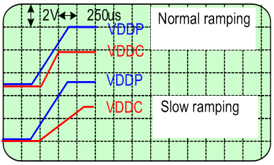
Figure 1: Different Ramp-up speed
Figure 2 shows the expected MCU in-system power-up behaviour vs. changes of the input voltage, specifically the PAD logic and peripherals.
Note: The behaviour may vary from product to product.
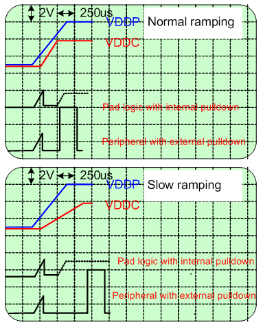
Figure 2: MCU in-system power-up behavior vs. changes of the input voltage
1) When the input voltage increases, the following behaviours are expected in sequence:
- PADs voltage will follow VDDP until pull-up/down device is activated.
- PADs voltage will ramp-up further.
- Firmware will be activated when EVR is ready.
- When firmware is initialized, clock system must be ready,
- User code is executed.
2) When input voltage to MCU drops from normal working voltage, the following behaviours are expected in sequence:
→ As long as EVR supports the internal logic:-
- Clock system output should drop with input voltage.
- Brown-out reset should not be triggered.
- PADs voltage is still in defined status.
→ If input voltage drops further, until EVR is not able to support internal logic:-
- Brown-out reset is triggered.
- Chip stops functioning.
- PADs go to RESET.
- VDDP drops further, PADs voltage might be in undefined status.
3. Low cost test set-up
To evaluate the power-up behaviour of MCU, the low cost test setup has been used, which is easy to setup and highly portable.
Figure 3 shows the brief overview of the test setup.
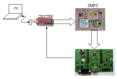
Figure 3: Test Setup Block Diagram
The setup consists of USB Tester, PCB board, host PC and the target DUT. The DUT can be based on any target MCU to be validated for its power-up behaviour.
The tester is an Ultra-Low-Cost evaluation platform consisting of several MCU’s. One of the MCU available on the platform is used to generate the PWM waveform. Various voltage ramp-up sequences can be generated with the tester coupled to the SMPS board. Figure 4 shows the circuit diagram of the SMPS board.
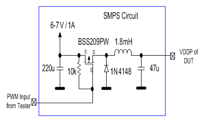
Figure 4: SMPS Board Schematic
For observation some of the DUT outputs can be connected to tester and feedback to the PC. Tester is associated with PC based monitoring tool which can be used to capture data/signal from DUT. The captured data can be displayed in real time on a soft oscilloscope, which gives us a quick overview of the evaluation result. The tool also allows simple commands to be sent directly to the target which enables user to choose different set of inputs without changing the tester code frequently.
Figure 5 shows the screenshot of PC-based monitoring tool. Using the control box some simple commands can be sent to the DUT, to control the ramp-up speed by changing the PWM duty cycle. The soft oscilloscope shown below is useful to monitor the MCU outputs.
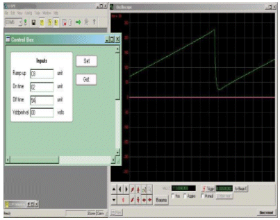
Figure 5: PC Monitoring Tool Screenshot
4. Test implementation
Test implementation is one of the important milestones for this approach. It is critical to define the possible and required input combinations in order to evaluate the MCU behaviour.
The combination of various VDDP ramp-up speeds and initial voltage conditions that affect the MCU power-up behaviour have to be defined first. Subsequently, one shall define the expected MCU behaviour and the tester response based on the predefined limitation. Also, the test implementation shall consider different MCU modules interconnections which might get affected by the changes in input voltage. These are some of the major considerations before the tests are implemented.
Figure 6 shows various input voltage patterns for the evaluation of power-up behaviour.
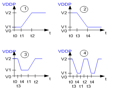
Figure 6: Various input voltage patterns for the evaluation of power-up behaviour.
Graph 1 and 2 show the simple power-up and power-down conditions, where the initial voltage of the power-up application may not be 0V under certain conditions. Graph 3 and 4 show the combination of different power-up and power-down patterns, where the MCU behaviour will be analyzed continuously under these conditions.
The timing t0 to t4 shown in Figure 6 refer to settling and rising time of VDDP. These timing could be defined based on test setup requirements, for example 10usec, 10msec, etc.
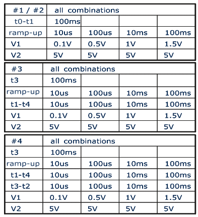
Table 1 summarizes the Figure 6, where #1, #2, #3 and #4 in below table refers to each graph shown in the above Figure 6 respectively.
Table 1: Combinations of VDDP Timings
- V1 is the initial voltage of the input supply;
- V2 is the final voltage level.
- t0-t1 is the settling time before ramp-up.
- t1-t2 is the ramp-up speed of the input voltage from the initial level to final level.
- t2-t3 is the ON duration of device (the delay between ramp-up and ramp-down)
- t3-t4 is the ramp-down speed.
- t4-t1 is the OFF duration of device (the delay between ramp-down and ramp-up).
As shown in above Table 1 with different VDDP ramp-up and ramp-down speeds, different initial voltages, different time intervals for continuous power-up, most of the critical cases will be covered under this analysis.
After the input voltage combinations are defined, the next step will be the software coding. Test code for the tester has to be developed in which the SMPS board will be controlled for different input’s simulation. PWM of the MCU is used for generating various input waveform. Tester configuration plays an important role in this test implementation for PWM waveform generation. Also the test scripts for DUT should be generated to analyze the target MCU behaviour.
In order to observe PAD behaviour and firmware flow, one of GPIO pin of DUT is designed as pull down logic enabled by default. When the firmware is initialized, this pin’s pull-down logic will be disabled. In the test setup, this pin is connected to an external pull-up resistor which will give clear indication when the PAD logic starts to work, and when the firmware ends. A timer will be configured to observe the clock system behaviour. This can be done by continuously observing the PWM duty cycle.
5. Results
Using the above described test setup and the various ramp-up/ramp-down conditions, one of the latest MCU was evaluated. The results shown below are the observed power-up behaviour.
The following combinations of inputs can be generated:
- VDDP ramp-up speeds : 100us, 10ms, 100ms,
- Initial voltages: 0.1V, 0.5V, 1V, 1.5V.
- VDDP ramp-down speeds: 10ms, 100ms.
With different VDDP ramp-up speeds, subsequent figures below show the behaviour of:
- VDDC
- PAD logic
- Firmware flow
- Clock system
With reference to the expected behaviour, following are the interpretations from the above waveform:
- The GPIO voltage follows the VDDP at the beginning, until pull device is activated pad logic is fighting against external pull-up.
- When EVR is initialized, GPIO voltage goes up to VDDP to indicate that the firmware is active.
- As VDDP input continues to rise, user code is executed. The clock system can be analyzed by the 48 KHz PWM.
Figure 8 & 9 show the waveforms for 10ms of VDDP ramp-up and 100ms VDDP ramp-up respectively.
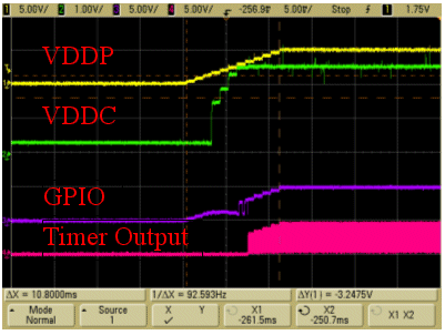
Figure 8: VDDP Ramp-up speed 10ms
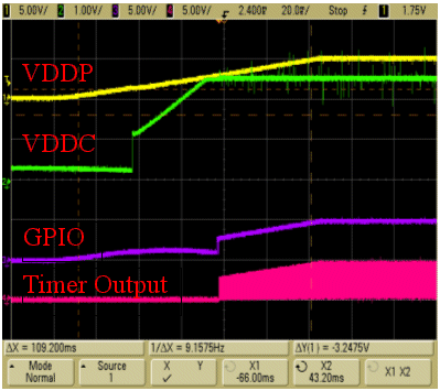
Figure 9: VDDP Ramp-up speed 100ms
The observation shows that with these 3 different VDDP ramp up speeds, the DUT can still maintain the normal function, which doesn’t show any failures. It shows that the timing for PAD logic, firmware flow and delay for user code to work will be affected. The clock system behaviour will not be affected by different VDDP ramp up speeds.
With this test setup and test code implementation, the measurement can also be done for different stages within power-up procedure. This helps the customer to do the application.
For VDDP ramp-down test, 10ms and 100ms don’t make much difference to the device behaviour. Figure below shows the 10ms ramp-down measurements.
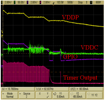
Figure10 VDDP Ramp-down speed 10ms
If the DUT is not power-up from 0V but at certain initial voltage, the timing of PAD logic and firmware flow with reference to VDDP level will be delayed, but the timing from PAD logic getting active to firmware flow getting active still remains the same.
6. Limitations
In the test setup, features of the tester MCU listed below will determine the ramp-up voltages:
- Clock : Maximum clock possible is 24Mhz
- Timer: Lowest possible timer resolution is 42nsec, due to the clock limitation
- Stability of the duty cycle of the timer peripheral also needs to be considered.
Due to the above limitation, 10us VDDP ramp-up speed could not be achieved. Besides, it is also not possible to generate the 100us and 10us ramp-down speeds.
Although there are some limitations, this low-cost setup helps to get a quick overview of the DUT power-up behaviour for around 50% of the ramp-up combinations before the complete analysis can be performed.
7. Conclusion
With this setup, one of the latest microcontrollers has been evaluated. Results show the setup is reliable, and can be used as the complimentary setup to the conventional huge and expensive test equipment. This setup can be easily reused on all other microcontroller power-up behaviour evaluation.
Low cost and portability makes this approach unique!
8. Terminologies
- MCU- Microcontroller Unit
- DUT- Device Under Test
- EVR- Embedded Voltage Regulator
- PWM- Pulse Width Modulator
- SMPS- Switch Mode Power Supply
- PCB- Printed Circuit Board
- USB- Universal Serial Bus
- VDDP- PAD supply voltage
- VDDC- Core supply voltage
Related Semiconductor IP
- Voltage and Temperature Sensor with integrated ADC - GlobalFoundries® 22FDX®
- 8MHz / 40MHz Pierce Oscillator - X-FAB XT018-0.18µm
- UCIe RX Interface
- Very Low Latency BCH Codec
- 5G-NTN Modem IP for Satellite User Terminals
Related Articles
- Selecting an embedded MCU: How to avoid evaluation trap?
- Performance Evaluation of machine learning algorithms for cyber threat analysis SDN dataset
- Memory Prefetching Evaluation of Scientific Applications on a Modern HPC Arm-Based Processor
- Microcontroller Applications -> 'Internetworking' treads on MCU turf
Latest Articles
- SNAP-V: A RISC-V SoC with Configurable Neuromorphic Acceleration for Small-Scale Spiking Neural Networks
- An FPGA Implementation of Displacement Vector Search for Intra Pattern Copy in JPEG XS
- A Persistent-State Dataflow Accelerator for Memory-Bound Linear Attention Decode on FPGA
- VMXDOTP: A RISC-V Vector ISA Extension for Efficient Microscaling (MX) Format Acceleration
- PDF: PUF-based DNN Fingerprinting for Knowledge Distillation Traceability