FPGA prototyping of complex SoCs: Partitioning and Timing Closure Challenges with Solutions
Vijay Kumar Kodavalla, Nitin Raverkar
Wipro Technologies, Bangalore, India
Abstract
In the nanometer era, complex SoCs have higher risk of re-spins. Undoubtedly FPGA prototyping is the right way of pre-silicon SoC validation, accelerate system software development and to meet time-to-market demands. Today’s EDA tools are not matured enough to effectively tackle complex FPGA partitioning and timing closure issues. For successful FPGA prototyping, design partitioning and timing closure need to be skillfully handled. This paper presents partitioning and timing closure challenges along with effective schemes to resolve these issues. This paper is backed up with vast FPGA prototyping experience of various SoCs with logic gate count up-to four million.
1. Introduction
FPGA prototyping is a viable solution to address growing SoC development complexities and associated risks. The exciting benefits of FPGA prototype are:
- Concurrent Software development and testing: Quick fine tuning of hardware/software partitioning, software development and comprehensive testing before actual silicon
- Comprehensive Verification: Integrated hardware-software testing
- Field Testing: In-system device validation in end-application deployment scenario
Following are the objectives for FPGA prototype to be effective:
- System performance
- Optimal number of FPGAs
- Shorter turn-around cycle from bug fixed RTL to FPGA bitmaps with consistent results
Following are the limiting factors for achieving the objectives:
- System performance: Due to system software and interface requirements, prototype is expected to run at certain minimum frequency (e.g.: 30-40MHz for video processing chips)
- Available FPGA resources: Gates, Pins, memories, clocks and resets
- Unfrozen SoC RTL: Due to concurrent prototype development and RTL verification
- No SoC RTL customizations: RTL modifications are not desirable for FPGA prototype timing improvement
Partitioning and timing closure are major challenges in mitigating effects of the limiting factors and to meet the objectives. This paper presents limitations in today’s FPGA prototyping methodology in section 2. PTC (Partitioning & Timing Closure) challenges and effective techniques to resolve them are discussed in section 3. The section 4 highlights benefits obtained by applying PTC techniques on a sample complex four million logic gate SoC, followed by conclusions in section 5.
2. Limitations of current Prototyping Methods
Even after rigorously following FPGA prototyping flow using state-of-art EDA tools, following are the limitations:
- Many FPGAs are required for SoC partitioning, leading to prototype system complexity
- Unable to do TDM (Time Division Multiplexing) pin assignment due to stringent timing requirements
- Unable to partition multiple clocks and reset trees
- No correlation of synthesis , P&R [place & route] timing results and critical paths
- Post P&R, routing delay is 4 to 9 times of logic delay and frequency achieved is 3-4X lower than the target value
- Inter FPGA timing not met with long combinational paths including board delays
- Inconsistent timing results even with minor RTL bug fixes and enhancements
- Route delay estimates of Physical synthesis tool are inaccurate due to lack of target device physical characteristics knowledge, leading to only 0.1X performance improvement
Tactful planning and innovative PTC techniques need to be applied to handle these critical issues.
3. Critical Issues and Solutions [PTC]
The limitations of current prototyping methods listed in section 2 broadly fall into partitioning and timing closure categories. This section presents the critical issues in partitioning & timing closure and innovative ways to resolve them.
Figure 1 shows a sample SoC block diagram highlighting the bus structure.

Figure 1 SoC – System level block diagram
Knowledge of SoC architecture is a must to get clarity on internal bus structure and inter-module connectivity. Bus structure indicates a possible partitioning boundary while the inter-module connectivity indicates the pin count requirements. Knowledge of module level gate count gives an idea on modules that can be combined and helps in deciding type and number of FPGAs required.
The critical issues and solutions of partitioning and timing closure are tightly coupled. The discussed solutions need to be applied with state-of-art flows and EDA tools.
Challenge 1: Many FPGAs required
Solution: Based on application test requirement, determine whether all SoC modules are required concurrently on FPGA for validation. Usually all the SoC modules are not concurrently required to be prototyped. Hence different SoC subsets can be formed. Build a “concurrency matrix” as shown in Figure 2, which helps in arriving at optimal balance between number of SoC subsets and FPGAs required.
Assume that a SoC has different modules like Processor, DMA controller, Memory controller and other data processing engines like M1, M2 & M3. Depending on application test scenarios (A, B, C and D) different modules can be grouped together, which demands concurrent verification. The modules required for each test scenario are shaded in Figure 2.
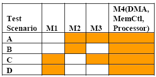
Figure 2 Concurrency Matrix
In this concurrency matrix (Figure 2), M1-M3- M4 or M2-M3-M4 needs to be concurrently validated. If the entire SoC is targeted to be validated in one go, then the total gate count is equivalent to sum of that of individual modules (M1+M2+M3+M4). In this example the SoC has been split into two subsets (M1-M3-M4 and M2- M3-M4). The worst-case gate count of these subsets will determine the number of FPGAs required. In this case the gate count to be considered for FPGA validation is equivalent to maximum of that of M1+M3+M4 or M2+M3+M4.
Lower number of FPGAs also reduces interconnect complexity. Also the RTL for various subsets can be easily done using “`if def” construct in top level RTL file.
Challenge 2: Selecting appropriate FPGA
Solution: Worst case gate count, memories, multipliers, DLLs, number of IOs and IO standards of the derived subsets drive the FPGA selection. The chosen FPGA logic gate count should be at least 30-40% higher as RTL might not have been matured at the start of prototype development cycle.
Challenge 3: Large number of IOs
Solution: A subset partitioning can start with the knowledge of module level area utilization, IO and clock requirements. The EDA tools will aid in performing interactive partitioning with “what if” analysis. Partitioning uncovers SoC internal large size buses and may demand more than available FPGA IOs. It is not always possible to do TDM of pins, as it brings down system speed. Before attempting TDM technique, apply logical solutions like:
- Common module logic distribution: Slice and place common modules (e.g.: register block) having many net connections to other modules such that their interconnections are reduced.
To elaborate this, refer to Figure 3 showing register block kept in a single FPGA and Figure 4 showing the sliced register block and its effect on interconnections.
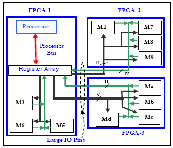
Figure 3 Common Register Block
For example, assume that the SoC logic is divided into three FPGAs with the concurrency matrix technique. The SoC register block (Register Array) is attached to processor through the processor bus. Output of register block has many configuration and control signals [v + n] to various modules of SoC named M1, M2, Ma, Mb etc. Similarly signals like status, interrupts and hand-shake signals [u + m] are the inputs to register block from various SoC modules.
Register block when placed in a single FPGA consumes more IOs [m + n + u + v] leaving almost no pins for rest of the module connections between FPGAs. Large IO requirement issue is resolved by slicing the register block. The sliced register blocks should be placed with its related modules (Figure 4). This will not have any adverse effect on timing as most of the register block connection to other modules carries static signals (false or multi-cycle paths), for e.g. configuration signals. Hence these signals are not timing critical.
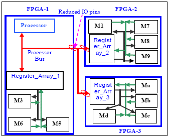
Figure 4 Distributed Register Block
- Functional based partitioning: In case partitioning leads to multiple data buses coming out of various FPGAs and getting multiplexed in one FPGA (e.g.: DMA Controller with one channel active at a time, as shown in Figure 5), slice and place the multiplexers as shown in Figure 6.
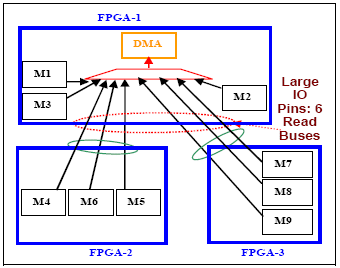
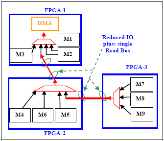
Figure 6 Partitioning – Distributed Muxes
Challenge 4: Partitioning Clock generator with multiple derived clocks
Solution: Use of PLLs, dividers, multiplexers and synchronizers in clock/reset generator of SoC complicates partitioning. Though dividers and multiplexers can be mapped to FPGA, the delay on these derived clocks will be high and may vary from run to run. The EDA tools are not able to perform IO timing analysis w.r.t derived clocks. To get a common clock reference for all the FPGAs, place the clock generator in one of the FPGAs as shown in Figure 7, bring out derived clocks and input to all the FPGAs as primary clocks. This also helps in getting correct IO offset timing analysis for derived clocks. In case of number of clocks exceeding available global clock lines, apply following techniques:
- Check if any clock domains can be merged
- Assign high fan-out clocks to dedicated clock tree in the device
- Assign relatively low fan-out clock nets to local low skew lines in the device
- Convert gated clocks to clock enable of Flops using advanced synthesis tools
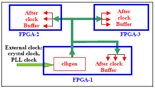
Figure 7 Clock Generator
Challenge 5: Partitioning Reset generator
Solution: Reset generator module will have reset synchronization logic to synchronize reset to each clock domain. The best way of handling reset generator module is to duplicate in all FPGAs as shown in Figure 8. Also if available, use dedicated low skew routing resources or device-wide dedicated reset resource.
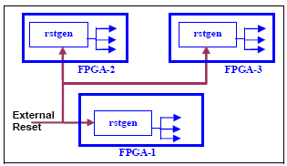
Figure 8 Reset Generator
After finalizing the FPGA partitioning, the next steps are Synthesis, Place/Route and timing closure. Analysis of synthesis report helps in estimating the frequency that can be achieved after P&R. The maximum FPGA prototype frequency can be achieved if routing delay can be brought down, which is almost equal to logic delay.
Challenge 6: Multiple iterations between Synthesis and P&R
Solution: The maximum FPGA prototype frequency achievable and limiting factors should be known upfront, before iterating between synthesis and P&R. In synthesis, meeting final target frequency is necessary but not sufficient condition as the route delay estimates are inaccurate.
In synthesis logic delay to be achieved for a given target frequency = 0.5*[(1/Target frequency) – off-chip delay (if any) + Clock skew]
Above equation is valid only when PTC techniques are applied. Current Synthesis tools don’t support constraining only logic delay. Hence manually check whether required logic delay is met in Synthesis for a given target frequency. If logic delay is not met in synthesis, achievable post P&R target frequency can be estimated by using above equation.
Synthesis tool features like register re-timing, logic replication and fan-out control can improve synthesis performance. Also in synthesis keep the hierarchy intact, which will help in P&R.
Challenge 7: Post P&R routing delay is more and intra-FPGA timings are 3-4X lower
Solutions: For complex designs with around 70% or more device utilization, it has been observed that post P&R routing delay is 80-90% of the overall delay. With these excessive routing delays, the final frequency achieved is 3-4X lower than target.
Various reasons for large routing delays are congestion, fixed position macros, paths traversing hierarchies and auto placement inefficiencies. Register block partitioning, reset mapping, device macros location fixing, module level floorplanning, “IOB Ring” pin locking and fan-out control are the techniques to control high routing delays.
IO pin locking, macro location fixing and module level floor-planning techniques:
- FPGA pin-out fixing has got major impact on the internal routing delays. It is inadequate to assign pin-out based on physical pin sequence in the BGA package. FPGA IO ring, which is present on periphery of FPGA die, needs to be considered while assigning pin-out
- In the floor-planning proximity doesn’t always guarantee good results, as the results depend on routing structure of the device
- Draw the data flow diagram of the SoC with the memories that are used to terminate the data paths
- Interdependent units should be closer by avoiding criss-cross and diagonal routes
- Place the Macros closer to the interfacing unit and constraint the Macro locations.
- The units which are not timing critical need not be floor planned there by P&R tool can have the flexibility in placing them
- Avoid overlapping regions and allow some free rows and columns between modules, which will aid in inter module routing
Challenge 8: Post P&R inter-FPGA timing issues
Solutions: To avoid any long combinational paths between FPGAs, partitioning should be always on register boundary. Also the solution for challenge-4 will ensure source synchronous inter-FPGA communication without sending clock along with data.
While driving out clock from FPGA to off-chip devices like DDR memory, use “clock forwarding” technique to match clock and data path delays. Figure 9 explains the clock forwarding technique using DDR IOs. In this the DDR data and clock path experiences equal amount of delay in IO.
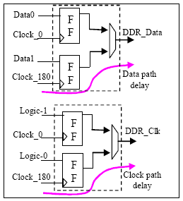
Figure 9 Clock Forwarding
Even with enhanced and bug fixed RTL, the PTC techniques ensure best and consistent results in every run.
4. Experimental Results
The example SoC design attributes are:
- 4M logic gates with 2M memory bits
- Targeted to run at 100MHz
- Maximum number of logic levels between Flop to Flop are 55
- Number of clocks: 24; Gated clocks: 200
The FPGA prototype frequency target is 27MHz. Table 1 lists results achieved by applying PTC innovative techniques.
Challenge Results with standard flow with state-ofthe art EDA tools Result/Benefits with PTC techniques 4 millionlogic gate SoC partitioning Number of FPGAs required = 5 (FPGA: 8M system gates with 1100 usable IOs) Number of FPGAs required = 3 with two downloads. 40% Reduction IO pins IO Pins required per FPGA = 1750 IO pins required per FPGA = 950 45% Reduction Intra-FPGA timing 12MHz 40MHz 3.33X improvement Inter-FPGA timing 10MHz 30MHz 3X improvement
| Challenge | Results with standard flow with state-ofthe art EDA tools | Result/Benefits with PTC techniques |
| 4 million-logic gate SoC partitioning | Number of FPGAs required = 5 (FPGA: 8M system gates with 1100 usable IOs) | Number of FPGAs required = 3 with two downloads. 40% Reduction |
| IO pins | IO Pins required per FPGA = 1750 | IO pins required per FPGA = 950 45% Reduction |
| Intra-FPGA timing | 12MHz | 40MHz 3.33X improvement |
| Inter-FPGA timing | 10MHz | 30MHz 3X improvement |
Table 1 Experimental results
5. Conclusion
Partitioning and timing closure challenges in FPGA prototyping of a complex SoC needs to be skillfully handled with PTC techniques at various stages of prototype development. Use of PTC techniques assures consistent results which helps in reducing the FPGA prototype development time.
We have demonstrated best results of FPGA prototyping by using innovative PTC techniques with minimal iterations and cycle time reduction. This paper will help in successfully meeting FPGA prototype objectives with predictive mapping and timing closure results.
6. References
[1] Taraneh Taghavi, Soheil Ghiasi, Abhishek Ranjan, Salil Raje and Majid Sarrafzadeh, “Innovate or Perish: FPGA Physical Design”, ISPD 2004.
[2] H. Krupnova, “Mapping Multi-Million Gate SoCs on FPGAs: Industrial Methodology and Experience”, Proc. DATE 2004.
[3] William Wu, Dr. Jim Tobias and Bob Uvacek, “Experiences with Multi-Core SoC Designs with FPGA Prototyping”, IEEE HPCA-11: Workshop on Architecture Research using FPGA Platforms, Feb. 2005.
[4] King Ou, “Using ASIC Prototyping to Reduce Risks”, SNUG, San Jose 2005.
[5] Gary Spivey, Shuvra S. Bhattacharyya and Kazuo Nakajima, “Logic Foundry: Rapid Prototyping of FPGA-based DSP Systems”, Proceedings of the Asia South Pacific Design Automation Conference, Japan, January 2003.
[6] Scott Hauck and Gaetano Borriello, “Logic Partition Orderings for Multi-FPGA Systems”, ACM/SIGDA International Symposium on Field- Programmable Gate Arrays, pp. 32-38, February, 1995.
Related Semiconductor IP
- NPU IP Core for Mobile
- NPU IP Core for Edge
- Specialized Video Processing NPU IP
- HYPERBUS™ Memory Controller
- AV1 Video Encoder IP
Related White Papers
- FPGA Prototyping of Complex SoCs: RTL code migration and debug strategies
- Complex SoCs: Early Use of Physical Design Info Shortens Timing Closure
- Bigger Chips, More IPs, and Mounting Challenges in Addressing the Growing Complexity of SoC Design
- Tackling large-scale SoC and FPGA prototyping debug challenges
Latest White Papers
- Ramping Up Open-Source RISC-V Cores: Assessing the Energy Efficiency of Superscalar, Out-of-Order Execution
- Transition Fixes in 3nm Multi-Voltage SoC Design
- CXL Topology-Aware and Expander-Driven Prefetching: Unlocking SSD Performance
- Breaking the Memory Bandwidth Boundary. GDDR7 IP Design Challenges & Solutions
- Automating NoC Design to Tackle Rising SoC Complexity