Fmax Margin/Value Improvement for Memory Block During ECO Stage
By Dhaval S. Shukla (eInfochips - An Arrow Company)
Abstract
The intent of this article is to explain how to fix Fmax margin/value during ECO stage using buffer/inverter-pair removal and push-pull techniques. Fmax for memory block shall be the Tcc limited. But due to over fixing the hold violation for few instances path, they become memory-limited, or SMS limited. In this article we will be discussing how to fix this in the ECO stage.
I. Introduction
The Engineering Change Order i.e., ECOs will be done for the following purposes:
- Change in functionality (Functional Eco)
- To fix timing violations (Timing Eco)
- To fix violations due to SI (SI Eco or Noise Eco).
Functional ECOs will fix any bugs detected during GLS or to modify the functionality of the design. Timing & SI ECOs will happen during the timing closure iterations in physical design phase.
Functional ECO
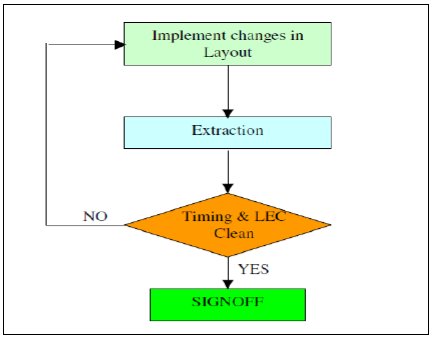
Functional ECO implements the changes in P&R tool by identifying the changes to the netlist with respect to the existing netlist. These changes may include
- Removal/Addition of cells and their connectivity.
- Changes in nets’ connectivity (may be in clock, signal paths).

Fig1: Functional ECO Flow Chart
While performing Functional ECO make sure timing & LEC passes after ECO implementation.
Timing and Noise ECO
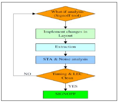
The Timing ECOs can include
- Fixing setup, hold, recovery, or removal, or max capacitance, or max transition, or Pulse-width, or Pulse Period violations.
- The Noise ECOs include fixing glitch propagation, which may cause functional failure of a chip.

Fig2: Timing ECO Flow Chart
While performing Timing ECO make sure timing & LEC passes after ECO implementation.
II. Fmax Condition and fixes
In a recent physical design project, I was working to improve the Fmax margin. Out of five blocks, three blocks were memory limited. This project was based on respin activity where we were not performing PnR again. Only memory ndm and timing db were updated plus mapping with new design reference libraries. Once respin was done, we performed Extraction and STA, followed by timing analyses.
After silicon validation, we performed this respin and checked fallouts in design. In a few blocks, there were minor fallouts in the hold and transition value. Which had been fixed in subsequent eco stages. While fixing hold at a few corners, Fmax value got violated by ~1 % to ~3%. i.e Few instances become memory-limited at some corners, which we need to make Tcc limited as per the project requirement.
Memory instances become memory-limited/sms-limited when the hold is over-fixed during timing closure by adding more buffers/inverter-pair in the data path. This degrades Fmax. i.e., setup. All memory instances in the block must be Tcc limited.
Below is the Fmax condition for the memory instances.
Tcc freq < Mem. R/W freq < SMS freq
We need to check if the margin is available or not.
- If Tcq< Tcc then there is a scop to fix Fmax.
- If Tcq > Tcc then there is no margin left to fix Fmax.
A] Removing Buffers/Inverter-Pairs from Datapath
First, we shall check the Tcq value and Tcc value, then decide whether buffers/inverter pairs are available in the data path to be removed to improve the Fmax.
We need to check the violated endpoint for the same instance group for which Fmax got violated.
report_timing –delay_type max –group <instance_group_clk_name>
If buffer(s)/inverter-pair(s) is/are not present in the data path to fix Fmax, then we can try the push-pull method (i.e., skewing) in the clock path.
B] Push-pull method
While applying the push-pull method, we need to check whether the hold margin is available for the nth path, and (n+1)th path. Plus we also need to check the setup margin for (n-1)th path as well. If the margin is available at the previous, current, and next path then we can insert a buffer in the clock path to improve Fmax.
- Start point of the nth path will be the End point of the previous path i.e. (n-1)th path
- End point of the nth path will be the Start point of the next path i.e. (n+1)th path
Note:
- Tcq is Tclk -> q timing arc of memory instance (i.e memory delay).
- Tcc is TC clock cycle.
- SMS is a Star Memory System which includes redundancy, scan, and BIST.
- TC means Testchip.
We could improve the Fmax value by 2% for two instances in one block for a particular corner where Fmax got violated but for other three instances in two blocks were having small Tcc-Tcq gap for a particular corner, which could not be fixed during further ECO stages, since it must be addressed during the syn-sta stage.

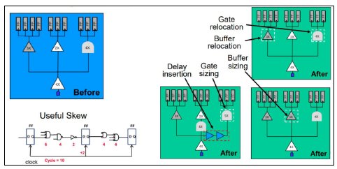
Fig3: Different technique to fix timing [Image Source: Adam Teman]
There are other techniques to fix Fmax like.
- using upsizing the cells (i.e., increase drive strength) in data path.
- replacing buffers with two inverters placing farther apart so that delay can be adjusted.
- reducing some larger than normal capacitance on a cell output pin; upsizing the cells to decrease the delay through the cell.
- usage of LVT cells in data path.
About the Authors
Dhaval Shukla
Dhaval Shukla is working as an ASIC Physical Design Engineer at eInfochips (An Arrow Company). He has more than 5.5 years of experience in ASIC Physical Design. He has experience in the bock level implementation at lower technology node (3nm, 4nm, 22nm and 40nm) for ASIC chip, where his accountabilities include the Block level PnR, ECO Implementation and Complete Sign-off Closure and for the same. He has handled multiple complex blocks in terms of memories, power blocks and instance count in the design. His project exposure also includes the flow implementation like merge, Fill and PV (i.e., Antenna, DRC and LVS).
Related Semiconductor IP
- 8MHz / 40MHz Pierce Oscillator - X-FAB XT018-0.18µm
- UCIe RX Interface
- Very Low Latency BCH Codec
- 5G-NTN Modem IP for Satellite User Terminals
- 400G UDP/IP Hardware Protocol Stack
Related Articles
- Pie: Pooling CPU Memory for LLM Inference
- A novel 3D buffer memory for AI and machine learning
- Efficient Hardware-Assisted Heap Memory Safety for Embedded RISC-V Systems
- Combating the Memory Walls: Optimization Pathways for Long-Context Agentic LLM Inference
Latest Articles
- SNAP-V: A RISC-V SoC with Configurable Neuromorphic Acceleration for Small-Scale Spiking Neural Networks
- An FPGA Implementation of Displacement Vector Search for Intra Pattern Copy in JPEG XS
- A Persistent-State Dataflow Accelerator for Memory-Bound Linear Attention Decode on FPGA
- VMXDOTP: A RISC-V Vector ISA Extension for Efficient Microscaling (MX) Format Acceleration
- PDF: PUF-based DNN Fingerprinting for Knowledge Distillation Traceability