DDR Memory Systems at the Heart of Consumer Electronics
Denali Software, Inc.
Courtesy of OCP-IP
In this article, DDR memory systems will be discussed in the context of consumer electronics design, with an emphasis on the need for a multi-disciplined, system-level approach. A brief look of relevant market pressures are followed by review of key issues in memory system development, including device selection, controller and PHY (Physical) design, and system integration. The article concludes with an example of commercially available solutions that address the key issues.
The Consumer Electronics Market
In today’s consumer electronics markets, it is not uncommon for designers to face a 6- month design window to achieve production within a 12-month window. One of the problems for designers in these consumer segments is that marketing simply does not know which features are going to be winners. As for the consumer space, dramatically changing feature sets are far more valued than performance, which is just one of the features in the set. The penalty for not getting the right set of features is a product that fails to find customers. The result is that about one-out-of-five products designed will actually get introduced to the market in the consumer space, and of these introduced products, only one in ten will have volumes in excess of a million units.
Data Hungry Consumer Products
One of the most significant factors in the success of today’s system-on-chip (SoC) designs is the ability to deliver efficient access to off-chip double-data-rate (DDR) dynamic random access memory (DRAM) memory. This is especially true in consumer SoCs where the memory subsystem is often shared, and must service numerous processing cores in the system, each with its varying bandwidth and latency requirements. In addition to providing data to multiple on-chip clients, the new multi-media-rich consumer products must now manage enormous amount of data while continuing to operate on an efficient power budget.
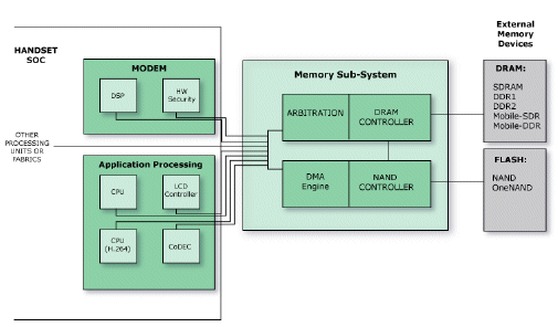
Consider a mid to low-end cell phone that consists of a digital baseband domain comprising a modem and an applications processor (See Figure 1). Within the modem, a DSP processes voice and data packets for the various cell phone communications strategies, GSM, CDMA, and the more recent 3G and 4G. The applications processor provides all the increasingly important GUI functions especially for video, image, and data. Next generation mobile devices include general-purpose CPUs, from providers like ARM, IBM, and MIPS as well as dedicated media processors for handling video encode and decode and 3D rendering for games. All of these processors have one significant bottleneck—the memory subsystem

Figure 1. Simplified Mobile Phone Diagram with Memory Sub-System
Five blocks make up the memory and storage subsystem of a mobile device:
-
Modem DSP code memory: NOR flash; SRAM, PSRAM, Mobile SDR/DDR with Flash companion chip for booting.
-
Modem DSP data storage: embedded-SRAM, SRAM, PSRAM, Mobile SDR/DDR.
-
Application processor code memory: NOR flash; SRAM, PSRAM, Mobile SDR/DDR with flash companion chip from which to boot.
-
Application processor temporary data memory: On-chip SRAM, SRAM, PSRAM, DDR2, and Mobile SDR/DDR.
-
Mass storage to contain large files like images and video: Mobile DDR DRAM, NAND Flash, and potentially small form factor hard disk drives (SFF-HDD).
DDR DRAM Controller Functionality
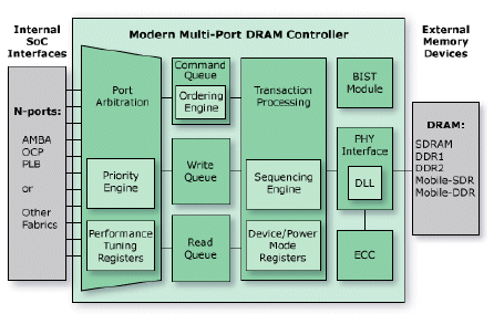
As a result of this bottleneck, modern DDR DRAM controllers (See Figure 2) have become quite complex, and are often implemented as fully pipelined designs with flow control for commands and data, where the goal is to maximize performance by allowing transactions to occur on every cycle. More complex controllers also support command reordering with built-in sequencing engines that optimize transaction cycles and latency, while maintaining relative priority and memory coherency. Combined with sophisticated multi-port arbitration functionality, these “data routing” features in the DDR controller block represent the key elements for efficiently serving data from memory to the various on-chip functional blocks. And because the memory controller is aware of all memory utilization variables—latency, bank activity, and command pipeline—it can optimize memory accesses for all the various computing modules.

Figure 2: DDR Memory Sub-system
Another critical element for the DDR memory subsystem is the ability to communicate with other storage systems, such as NAND Flash in a mobile phone design. For example, capturing high-resolution pictures and streaming video requires large amounts of highbandwidth storage. An efficient DDR memory system can enable direct transfers of these multimedia packets from the mass storage Flash devices into the DRAM, keeping unnecessary traffic off the main bus and increasing system performance. This functionality frees up the system busses for other tasks and reduces the overall power used for data transfer.
Memory System Interfaces
On one side, the DDR memory controller must interface with the design, usually through a standard bus interface or data fabric like AMBA, OCP, or PLB. The controller must be designed to deliver the appropriate Quality-of-Service (QoS) to processor, DSPs and graphics engines or other fabrics through one or more ports that comply with one or more of these standards. On the other side, the DDR controller must interface to memory devices through the PHY interface, which converts digital signals and commands from the memory controller logic into real-world, properly-timed waveforms that memory devices can interpret. This interface can be particularly challenging since PHY designs often include hardened or fixed components which are tightly coupled with process and library technologies, especially at frequencies in excess of 400MHz. The controller and PHY require uniquely different engineering skills, tools and methodologies, and thus, are often developed by separate engineering teams, or are acquired from different third-party design intellectual property (IP) vendors. Consequently, the lack of a standard interface between the two design elements has become the source of significant integration and verification costs by systems developers, memory controller vendors, and PHY providers.
Memory Device Options
In addition to the wide variety of memory device options, such as SDR/DDR DRAM, Mobile SDR/DDR DRAM, NOR/NAND Flash, PSRAM, etc., each device contains vendor-specific features, functions, and timing. Besides selecting the ‘right’ mix of device types for the application the memory subsystem must be designed to extract the necessary performance from those devices. Of course, the ‘right’ set of devices can (and most likely will), depend upon memory device economics (price, supply, availability), and marketing requirements (power, performance) for the end-product. These independently changing factors are a key driver for incorporating device-level configurability and programmability into the logic design for DDR memory systems. Programmable features are features which are usually controllable through a register in the design, as in Control-Status Registers (CSRs), whereas configurable features represent key functionality which can be easily included or excluded from the design, with little or no affect on the remainder of the system. In the case of NAND Flash, a well designed hardware abstraction layer can also enable configurability, and reduce firmware development time as well as increase firmware portability through the use of more generic drivers.
Design for Configurability and Programmabilty
It is easy to see that configurable and programmable memory systems, especially for consumer applications, are increasingly becoming a requirement in order to address market needs. However, developing reusable designs or IP blocks requires significantly greater investment in design and verification. As the number of features grow, adding a new feature to the design also presents unique challenges, especially in the verification domain. Each new requirement can double the configurable space, and if the requirements are an enable/disable-type of feature, the requirements resulting in multiple modes can increase the configurable space geometrically. Investment in the type of IP design and verification infrastructure that can deliver the necessary feature flexibility, while tracking changing memory architectures and economics, is largely impractical for most companies, with the exception of 3rd party IP vendors who can amortize cost across a much larger design base.
System-Level Memory Solutions
For most chip design efforts, 3rd party IP solutions are the accepted, and arguably necessary, solution for deploying other complex SoC interfaces such as PCI Express, USB, and Serial ATA. And while the protocol complexity of DDR memory systems is replaced by complexity in device market dynamics and non-standard PHY interfaces, there are proven IP solutions that address the system-level design of DDR memory systems. Developers have begun to realize significant productivity gains through reusable IP for DDR memory systems.
Denali DDR Memory Solutions
Configurable IP
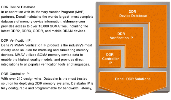
Denali Software is a leading provider of commercial DDR memory systems solutions, (See Figure 3) and has achieved a market leading status with over 210 design wins in the consumer, computing, and communications markets. One of the keys to this success is providing customers with a solution that incorporates the roadmaps for SoC performance, memory device technology, and silicon processes into a high-quality and repeatable solution for generating memory systems that meet system requirements. Customerspecific configurability is achieved through a patented IP infrastructure that converts device and system performance requirements into machine readable specifications that drives consistent, high-quality IP production from common code base. The overall IP generation process leverages Denali’s memory modeling products and the eMemory.com device database in an advanced SystemVerilog environment for RTL design and verification. Deliverables include: RTL and synthesis scripts, silicon-independent DDR PHY or DFI compliant PHY interface, verification testbench, static timing analysis (STA) scripts, programmable register settings, and documentation. Databahn controller supports multiple system ports, including AMBA, OCP, and PLB, with various configurable arbitration schemes.

Figure 3: Denali Memory Solutions
Memory Device Information
Providing customers with the most up-to-date information on memory device technology, product roadmaps, vendor capability, and second sourcing, is a key element of the overall DDR system solution. In cooperation with its Memory Vendor Program (MVP) partners, Denali maintains the world’s largest, most complete database of memory device information at eMemory.com. The eMemory.com database provides access to over 10,000 memory models and datasheets, covering all the latest DDR2, DDR3, GDDR, and mobile DRAM devices. Denali also maintains in-house market research resources for product development and customer engagements, and produces a public memory report which addresses key business and technology issues in the memory industry. In addition, Denali hosts the industries largest conference series, MemCon, which is sponsored by leading memory vendors and attracts thousands of designers at world-wide venues.
DDY PHY Development
The DDR PHY is also a key element in the overall DDR system solution. In addition to providing its own DDR PHY, Denali recently led a new industry effort to define a common interface between DDR memory controller logic and DDR PHY interfaces in order to reduce design inefficiencies and increase the potential for reuse of the PHY and controller components that make up DDR memory subsystems. The DFI specification is now in the final stages of development by expert contributors from recognized leaders in the semiconductor, IP and electronic design automation (EDA) industries, including: ARM, Denali, Intel, Rambus, Samsung, and Synopsys, and can be obtained at: www.ddrphy.org.
Summary
In addition to erratic and shrinking market windows, consumer electronics bring numerous other challenges to system designers. The rapid increase in data and multimedia, processing requirements in consumer electronics products has driven significant complexity in the associated memory subsystems. The effort to meet these increased performance and complexity requirements must also be addressed in the context of an independently changing roadmap of available memory device technologies. The task of producing efficient memory systems now requires tight synchronization of efforts spanning controller design and tuning, device and market intelligence, and silicon process roadmaps. Third-party solution can offer compelling solutions for repeatable and costefficient success if they address the complete solution. Denali is a pioneer in memory system design and verification, and offers market proven solutions for deploying DRAM memory subsystems for a wide range of end products and applications.
Related Semiconductor IP
- AMBA AHB Bus to DDR SDRAM Controller
- DDR SDRAM Controller
- DDR and DDR2 SDRAM Controller Intel® FPGA IP Core
- DDR and DDR2 SDRAM Controller with ALTMEMPHY Intel® FPGA IP
- DDR Encrypter
Related White Papers
- Revolutionizing Consumer Electronics with the power of AI Integration
- MIPI in next generation of AI IoT devices at the edge
- The Future of Safe and Secure Aerospace Systems
- Handling the Challenges of Building HPC Systems We Need
Latest White Papers
- Ramping Up Open-Source RISC-V Cores: Assessing the Energy Efficiency of Superscalar, Out-of-Order Execution
- Transition Fixes in 3nm Multi-Voltage SoC Design
- CXL Topology-Aware and Expander-Driven Prefetching: Unlocking SSD Performance
- Breaking the Memory Bandwidth Boundary. GDDR7 IP Design Challenges & Solutions
- Automating NoC Design to Tackle Rising SoC Complexity