Advancing Transaction Level Modeling -- Linking the OSCI and OCP-IP Worlds at Transaction Level
Pete Hardee, Director of Services and Strategic Marketing, CoWare, Inc.
Abstract:
The growing need for Transaction Level Modeling (TLM) standards that can link together SoC architecture and software development at levels of abstractions higher than RTL has stimulated CoWare and Sonics to collaborate on a cohesive methodology that addresses both SoC designer and software developer needs. This paper outlines the two prevalent industry approaches from OCP-IP (Open Core Protocol – International Partnership) and OSCI (Open SystemC Initiative) and then describes how two founders of both of these organizations are collaborating to provide real solutions to the industry. CoWare is an OCP-IP Sponsor member and founder of OSCI. Sonics is a co-founder of OCP-IP and contributor to the OCP-IP System Level Design Working Group.
The convergence of communications and multimedia data processing onto a single chip continues to push SoC complexity in two areas, SoC integration and software development. To address SoC integration issues, the industry has been moving towards standardizing the IP core interfaces to achieve high reuse. To address software development, the industry has been adopting higher abstraction simulation models which can deliver near enough performance and accuracy to enable software development to begin in parallel with chip development. While OSCI has focused on the software development concerns, and OCP has focused on SoC integration concerns, the concept of Transaction Level Modeling would most benefit from a methodology such that both standards can be utilized in a straight forward manner.
Using CoWare’s ConvergenSC and Sonics’ SMART interconnects; the two companies have designed such a common methodology which achieves the unified TLM goal. In this article, each TLM standard is discussed, followed by the interoperability work conducted between CoWare and Sonics.
In this article, we introduce both the OSCI and OCP-IP variants of TLM, outline CoWare’s contributions to help interoperability between them, and introduce the CoWare/Sonics development to provide SoC integration and software development solutions based on Sonics SMART Interconnects, with OCP interfaces, and CoWare’s ConvergenSC™ SystemC-based design environment.
1 TLM in SystemC – The OSCI Proposal
The primary goal of TLM is to dramatically increase simulation speeds, while offering enough accuracy for the design task at hand. The increase in speed is achieved by the TLM abstracting away the number of events and amount of information that have to be processed during simulation to the minimum required. For example, instead of driving the individual signals of a bus protocol, the goal is to exchange only what is really necessary: the data payload. TLM also reduces the amount of detail the designer must handle, therefore making modeling easier. The necessary information is presented to the designer as a TLM API (Application Program Interface).
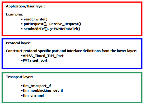
The OSCI TLM API is built as a set of interfaces that define how models communicate. These interfaces can be used in their primitive form, or augmented with a ‘protocol-layer’, which will target the basic interfaces to a specific on-chip communication protocol or design task. This protocol layer provides a set of convenience functions that make the TLM modeling abstraction much easier to use (see Figure 1).

Figure 1: Layered TLM API's
The API’s can be used in a range of abstraction levels depending on the amount of timing information required, and therefore included. The OSCI TLM working group uses the following terminology to describe these levels:
1.1 Programmers View (PV)
This is intended to imply a pure function call based interface with no communication events and little timing information carried. It is usually associated with Untimed Functional (UTF) behavior description.
1.2 Programmers View with Timing (PV+T)
A modeling style where a PV and a signal or FIFO interface co-exist – effectively the simulation can switch between two interfaces, with and without timing. The PV interface may be driven from a functional behavior model and the more accurate interface may be driven from a trace of the internal state of the functional model. The goal of this PV+T style is to allow model refinement without changing the functional description of the model’s behavior.
1.3 Cycle Callable (CC)
This is essentially a cycle accurate modeling style. The cycle-by-cycle behavior of the interface is explicitly described. The behavior of the model coupled with this interface would also include cycle timing – either a “cycle-count-accurate” Timed Functional (TF) model or fully cycle-accurate. Alternatively, the behavior may be omitted or modeled in a very trivial manner to create a cycle-accurate performance model. The CC level is still a TLM abstraction, distinctly above RTL, since the interface uses higher level ports rather than pin-accurate RTL signals. Also, multiple signal activity occurring on the same clock edge can be bundled together to create “transfers”, thus providing improved simulation performance compared to RTL.
2 TLM in SystemC – The OCP-IP Proposal
The OCP-IP TLM proposal provides an SoC communication modeling framework and is an output of the System Level Design Working Group within OCP-IP. The proposal comprises a set of well described layers of abstraction that together create a structured link between up-front architecture exploration and SoC implementation.
An additional objective is to create a hierarchy of models that are re-usable from one layer of abstraction to the next and across uses (e.g. performance analysis and testbench creation). Finally, the proposal is intended to provide clearly articulated entry points into the hierarchy from which EDA vendors, chip designers and architects can create and easily distribute tools, testbenches, executable specifications, and the like, within their organization or the industry as a whole.
2.1 Message layer (L-3)
Message, or Layer 3, models are at the highest level of abstraction defined and are intended to be used by SoC architects as proof of concept tools, to rationalize first order functional partitioning and to provide data needed to make system level architectural trade-offs. SoC models created at Layer 3 are also intended to be re-used as executable specifications.
L-3 models are event driven and untimed. Each transfer across their interface contains several datum that are often abstracted to a higher order. For example, a message could contain the equivalent data from several bursts of data at a lower level of abstraction that form a complete MPEG4 macro-block. Another key characteristic of this models created at this level of abstraction is that they are not address mapped, but process mapped.
2.2 Transaction Layer (L-2)
Transaction, or Layer 2, models are designed to be used by SoC architects to carry out detailed hardware performance analysis and hardware/software partitioning and co-development. They also contain a high degree of versatility in their application. They can be used to interface low level drivers with hardware simulation models, and integrate Operating System simulators with hardware emulators. Continuing the re-use objective, Transaction Layer models can also be used as the source for “Golden” test patterns and can form the test bench for Transfer Layer (L-1, below) models.
L-2 models have structural accuracy sufficient to model a complete system (address information and communication constraints), an event-driven computational model with approximate timing, and are highly parameterizable. Each transaction contains a transfer of several datum, such as a burst to memory, is OCP specific but is independent of any bus fabric protocols.
2.3 Transfer Layer (L-1)
Transfer, or Layer-1, models are designed to be used by designers to perform detailed modeling tasks that do not require accuracy down to the per interface signal level. They can be used for modeling the interfaces of embedded processors, creating cycle accurate test benches and carrying out cycle accurate performance simulations. They can also be used to perform equivalent performance comparisons with RTL objects.
L-1 models are clocked cycle-accurate. While interface pins are abstracted away, they follow interface protocols which are mapped onto the chosen hardware interface and bus structures. Each Transfer Layer transaction contains a single data item which is byte-accurate. The below table provides a simple chart showing some functional equivalents when moving from an RTL Layer model to a Transfer Layer model.
| RTL LAYER (L-0) | TRANSFER LAYER (L-1) |
| A single wire | A complete communications interface |
| Signals | Events, variables and functions |
| Interface signal interaction | Channel function calls |
2.4 RTL Layer (L-0)
For a point of reference, RTL, or L-0 Layer, models are both pin and bit accurate. They are also register transfer accurate and are written in VHDL, Verilog or synthesizable SystemC. Finally, estimated propagation timing can be back annotated.
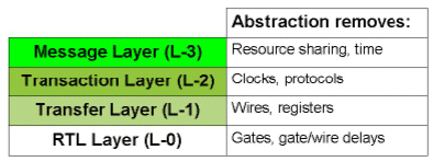
The OCP-IP System Level Design Working Group white paper entitled SystemC based SoC Communication Modeling for the OCP™ Protocol should be referred to for more detail. Figure 2 below illustrates the successive levels of detail that is removed at each level of abstraction.

Figure 2: OCP TLM Abstraction Levels
3 Working Towards Interoperability – Task-based TLM
As we have seen, both OSCI and OCP-IP define three levels of TLM. The naming convention used by OCP-IP for the different layers (Message, Transaction and Transfer) is based upon the granularity of the communication taking place between respective SystemC models simulated. This is very useful, and satisfies the original intent, as an SoC architect or designer can quickly understand the trade-off between relative simulation speed and communication detail and accuracy retained in the modeling scheme considered. However, only one of these six levels is clearly named based upon the design task for which the particular modeling level would be used – OSCI’s Programmers View. At CoWare, we decided to follow this idea through – to define three levels, consistently named for the appropriate design task, and allowing the maximum amount of commonality between the two sets of almost equivalent modeling proposals.
3.1 Programmers View
The Programmers View fills the need for a functionally correct model of the SoC and enables embedded software programmers to develop real-time applications and firmware. Large amounts of software need to be run for system testing, but on the other hand most of the hardware-related aspects can be ignored. Timing should be considered on a different scale than typically used by hardware and verification engineers, or could be absent all together. For a software developer, it is important to have the memory map correctly modeled, so a PV model will focus on that aspect – hence it could be termed “register-accurate”. OSCI’s work around the PV layer is quite well-defined, while OCP-IP’s work to date has not greatly focused on the Message Layer (L-3), which could be placed at a slightly higher level of abstraction than PV from a software developer’s perspective as an accurate memory map is not a requirement. CoWare’s own work in this area has largely followed the OSCI proposed standard. The CoWare PV solution is already finding application in customers’ projects, and is developing both high utility and maturity.
3.2 Architects View (AV)
The Architects View provides a model that allows SoC architects to identify and resolve potential bottlenecks, to make macro- and micro-architectural optimizations in hardware and software. Questions to answer are the number of processors and how to best partition software functions between them, what on-chip and off-chip memory hierarchies to employ, and what interconnect approach can deliver the required communication bandwidth and quality of service to all. For this purpose, architects need to analyze the SoC in different operating conditions, thus placing high expectations on simulation speed. A model used by architects may require functional models of all elements in the system, or alternatively some performance models (also known as “load models”) and traffic generators may be used. All models require sufficient timing information to analyze the performance of different architectures. In the OSCI TLM working group, this modeling level is known as PV+T, since it can be derived from the PV model by adding timing information. For OCP, this is the Transaction Layer (L-2). In contrast to the PV level, OCP has focused on this level considerably, and OSCI’s work is less mature and complete. CoWare has been working for some time with Sonics to complete a Transaction Layer L-2 solution for mutual customers and is described later. While CoWare will continue to work with specific customers using the PV+T level, we believe that the OCP L-2 layer is more generally useful and applicable.
3.3 Verification View (VV)
The Verification View enables verification engineers to use the system level models as testbenches to validate implementation of the different hardware blocks in the system. For this purpose they need to be able to interface the system level models with detailed HDL models and verify correct behavior at a cycle-accurate level. In the OSCI TLM working group, this modeling level is known by its implementation-oriented name of CC (cycle-callable). In OCP, this is the Transfer Layer (L-1). These levels are really quite closely equivalent. CoWare has had an equivalent level of cycle-accurate TLM available for a considerable time, with design-proven models in use with a high number of customers. We have recently focused on ensuring that our models can be built as an implementation on top of either OSCI CC or OCP-IP L-1 fundamentals.
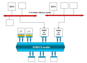
In addition to the work mentioned above, CoWare is working with OCP-IP to create models to bridge the OCP-IP and OSCI worlds. As a result of this, it is possible to efficiently mix many different IP models in the same design. This is shown in Figure 3, where two AMBA AHB-based sub-systems are shown connecting to an OCP/Sonics sub-system via AMBA-OCP bridges.

Figure 3: Mixed AMBA/OCP System
4 SMART Interconnect for the ConvergenSC™ SystemC-based Design Environment
One of the biggest efforts to link the SystemC and OCP worlds has been undertaken by Sonics and CoWare, at the request of mutual customers. To meet the growing levels of SoC complexity and the amount of interaction of large on-chip data flows, a sophisticated on-chip interconnect is required for any hope of meeting performance goals reliably within the market windows available. Sonics’ SMART Interconnects provide the only commercial solution to these growing problems. To further facilitate the development of SoC’s and their subsequent systems, Sonics is now producing SystemC models for all of their SMART Interconnect products, at either OCP layer L-1, or L-2 abstractions. For example, one particular major semiconductor vendor is using SiliconBackplane III and MemMax models at L-2 abstraction to model digital multimedia data flows and write system level software. Sonics and CoWare are collaborating to make these models available in a joint flow, which combines the power of the ConvergenSC tools for ESL design, with the versatility of the SonicsStudio™ tools for exploiting SiliconBackplane III’s extraordinary configurability. The joint design flow is illustrated in Figure 4. All models are instrumented for ConvergenSC’s analysis capabilities, allowing the platform architecture to be optimized, and the interconnect to be reconfigured with SonicsStudio. The L-2 models run fast enough to validate the system with large quantities of embedded software, while the tight links to SonicsStudio ensure decisions made in the SystemC domain are carried directly to the RTL domain within the configuration of the SMART Interconnect. The close links to the physical implementation of the interconnect then facilitate a first-time-right implementation that meets all necessary system requirements such as guaranteed Quality of Service (QoS). This tight integration of the two development environments ensures that decisions made in the SystemC domain are carried through to the RTL domain faithfully, removing any chance for translational error.

Figure 4: ConvergenSC-SonicsStudio Design Flow
5 Conclusion
Due to the exponential rise in the complexity of SoC’s and the amount of software to be executed on them, the need for higher levels of abstraction through SystemC modeling is clear. In order to reduce industry wide costs in developing the necessary infrastructure, and the need for reliable interoperability of models and environments, open industry standards are not only needed, but required. Both OCP-IP and OSCI have carried out important work to move the ball forward significantly in these regards. CoWare and Sonics are at the forefront of this work, which we believe to be fundamental for successful Electronic System Level design. One unified standard supported by all would be the ideal case, but we fear that there is already too much legacy investment for that to realistically occur. However, leveraging off this body of work, we believe that the joint CoWare/Sonics SystemC modeling offerings, driven by leading semiconductor and system OEM customers, will provide the optimal solution for SoC and system level success. Ensuring chip level and Electronic System Level design requirements are met, IP has maximum re-usability and ever shortening market windows are consistently hit.
Related Semiconductor IP
- NPU IP Core for Mobile
- NPU IP Core for Edge
- Specialized Video Processing NPU IP
- HYPERBUS™ Memory Controller
- AV1 Video Encoder IP
Related White Papers
- Transactional Level Modeling (TLM) of a High-performance OCP Multi-channel SDRAM Memory Controller
- Functional Transaction Level Modeling simplifies heterogeneous multiprocessor software development
- The 'what' and 'why' of transaction level modeling
- Transaction Level Model of IEEE 1394 Serial Bus Link Layer Controller IP Core and its Use in the Software Driver Development
Latest White Papers
- Ramping Up Open-Source RISC-V Cores: Assessing the Energy Efficiency of Superscalar, Out-of-Order Execution
- Transition Fixes in 3nm Multi-Voltage SoC Design
- CXL Topology-Aware and Expander-Driven Prefetching: Unlocking SSD Performance
- Breaking the Memory Bandwidth Boundary. GDDR7 IP Design Challenges & Solutions
- Automating NoC Design to Tackle Rising SoC Complexity