A Low-Power 16-channel AD Converter and Digital Processor ASIC
and R.Esteve-Bosch, B.Mota, L.Musa, A.Jiménez-de-Parga from CERN Geneva
Abstract
The extreme particle density in the detectors for highenergy physics experiments set new demands on the readout electronics in terms of resolution, density and power consumption. These requirements are beyond the present capability of commercial-off-the-shelf components and call for ASICs that embed in a single chip the circuits to digitise, process, compress and store the information of a high number of channels. In this paper we present an ASIC that responds to these needs, including in a single chip 16 low-power 10-bit 25-MSPS A/D converters, a data processor and 800-Kbit of memory. The chip, which is implemented in a 0.25 mm CMOS technology, has an area of 64mm2 and a power consumption of 320mW when the 16 channels are running at 10MHz rate. The measurements show a resolution better than 9.5 ENOB on all channels and a channel-to-channel crosstalk below –65dB. The techniques adopted in the front-end and back-end design of the circuit, to limit the impact of the digital noise on the ADC performance and the channel-to-channel crosstalk, are also presented.
1. Introduction
A new generation of high-energy physics experiments is in preparation at the CERN laboratories in Switzerland. A new accelerator, the Large Hadron Collider (LHC), will bring protons and heavy ions into head-on collisions at higher energies (up to 14 TeV) than ever achieved before. Four experiments are currently in preparation for initial operation in 2007. One of these experiments, ALICE (A Large Ion Collider Experiment) [1], is dedicated to the study of the collisions of several species of ions. The experimental apparatus to study the high number of various particles (up to 3x10⁴) produced in each collision, is a multi-component detector. Each component of the detector is used for measuring particle energy and momentum, and/or distinguishing different particle types. A central role in the ALICE detector is played by the Time Projection Chamber (TPC) [2], which provides a three-dimensional reconstruction of the particle trajectories.
The TPC consists of a cylindrical gas volume of about 90m3 under a uniform electrostatic field. Charged particles traversing the TPC volume ionise the gas along their path liberating electrons that drift towards the chamber endplates. At the endplates, conventional multiwire proportional chambers provide the charge amplification and readout by means of a cathode plane segmented in about 6x10⁵ pads. Each pad is connected to an electronics chain to amplify, digitise and pre-process the signal before transmission to the DAQ. The requirements for the front-end electronics and its basic architecture are discussed in [2, 3]. For every pad, the charge is integrated and subsequently shaped by a shaping amplifier. The pulse height spectrum over the TPC maximal drift length is stored as digital data. The front-end electronics has to satisfy many other constraints while meeting the required performance specifications. Mainly, the readout electronics needs to fit into the overall detector structure and, in particular into the available space, which is inaccessible while the experiment is running. This has important consequences in terms of integration density, long-term reliability, and power. In particular, the requirements for electronics with minimal dimensions, power and cost drive the integration density as high as possible. The unavailability of commercial components that integrate a high number of A/D converters and the need to combine A/D converters with a custom data processor have driven the design of the ALTRO (ALice Tpc Read Out) chip. Preserving the resolution of the standalone ADC was the major concern in the ASIC design.
2. ALTRO Architecture and Specifications
The type of signals to be processed by the ALTRO chip is a train of pulses sitting on a common baseline. The signals from 16 independent inputs are continuously acquired and processed. When the Level-1 trigger is received a predefined number of samples (acquisition) is temporarily stored in a data memory. If the Level-2 trigger is received, this acquisition is frozen otherwise it will be overwritten when the next Level-1 arrives. There is the possibility of having pre-trigger samples or to delay the acquisition by a programmable number of cycles.
As shown in figure 1, the ALTRO chip contains 16 acquisition channels each comprised of three main units: an ADC, a Digital Processor and a Data Memory. A short description of these three blocks is given hereafter.
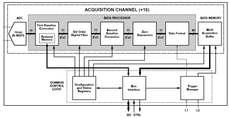
Figure 1. ALTRO Block Diagram
The ADC is the 10-bit 25-MSPS TSA1001 from ST Microelectronics. ST introduced recently a low-power ADC family [4] with 8, 10 and 12-bit units based on the same ADC structure. The TSA1001 offers the lowest power consumption with 25mW at 25-MSPS and 2.5V supply. A specific power-adaptive feature allows reducing this figure, when the ADC is operating at lower sampling rates, by means of an external polarisation current. The ADC has differential inputs with 1Vpp range and it is based on a pipelined architecture [5, 6, 7] with 1.5bit/stage as shown in figure 2.
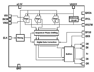
Figure 2. ADC block diagram
After digitisation, a Baseline Correction Unit is able to perform channel-to-channel gain equalisation and to correct for signal non-linearity and baseline drift due to temperature variations. It is also able to adjust DC levels and to remove systematic spurious signals by subtracting a pattern stored in a dedicated memory (Pedestal Memory). The next processing block is a 18-bit, fixed point, 3rd order IIR Digital Filter acting in the timedomain and whose function is described in [8]. A second correction of the baseline, based on a moving average filter removes non-systematic perturbations of the baseline that are superimposed to the signal. Eventually, a Zero Suppression module removes all data that is below a certain threshold, except for a specified number of pre- and post-samples around each pulse. When the pulses are closer than a given distance, they are grouped in the same data packet. This produces a certain number of non-zero data packets, thus, reducing the overall data volume. Each data packet is formatted with its time stamp and size information, so that the original data can be reconstructed afterwards.
The output of the Data Processor is stored in the Data Memory, which has a capacity of 5-Kbyte and is able to store 8 full acquisitions. The data readout is performed at 60MHz through a 40-bit wide bus, yielding a total bandwidth of 300-Mbyte/s. The ALTRO chip has two clock domains: 1) Sampling and Data Processing domain; 2) Data Memory readout and bus interface domain.
3. Implementation
The ALTRO chip is implemented in the ST 0.25µm HCMOS-7 process. Since the capacitors are implemented as a metal-to-metal sandwich, the ADC design does not require process options. This allows the chip to be manufactured in the plain digital process. The physical characteristics of the chip are summarised in table 1.
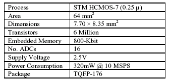
Table 1. ALTRO Physical Characteristics
The ADCs were placed in two blocks of 8 units each, mirrored in relation to each other. The memories for each channel were placed beside the corresponding ADC. The remaining fishbone-shaped area was used to place and route the processing logic using a flat approach. A detailed view is presented in figure 3.
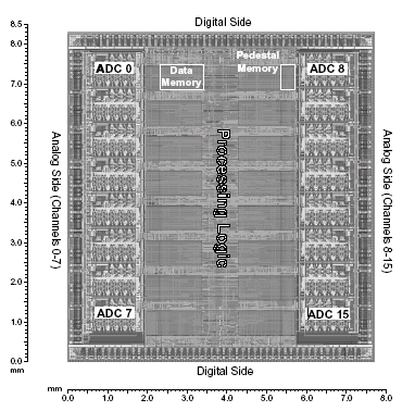
Figure 3. Layout of the chip
To reduce the effect of digital noise on the ADC, the following strategy was applied. Since 95% of the logic works on the sampling clock domain, the phase of the clock signal distributed to all the flip-flops can be adjusted such that the switching of all digital nodes occurs outside the conversion aperture-time of the ADCs. Each ADC block contains a passive clock tree balanced with the accuracy of 1ps. From the input pad, the clock signal is first split in two branches. One is manually routed to the 16 ADCs to ensure a skew of less than 5ps. The second one is distributed to all the processing logic. Since the depth of the digital clock tree is greater than that of the ADC clock tree, the clock edge reaches first the ADCs and then the digital logic. A margin of some 600ps, worst case, was taken. The aperture time of the ADC is 5ps and by the time the switching noise starts, the conversion is already done.
The location of the digital pads was selected based on noise and ground plane considerations and also to meet the routing requirements of the PCB. Thus, all the digital pads are placed on the top and bottom sides, including digital ground and supplies. The analogue pads are placed on the left and right sides, including analogue ground, supplies and the biasing of the ADC guard rings.
4. Characterisation of the Chip
Special attention has been paid to the characterisation of the ADC in order to know how the integration would affect its performance compared to the standalone part. For physics applications, the most relevant parameters are ENOB, DNL, INL and crosstalk. The measurement of these parameters is presented in Table 2.
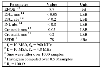
Table 2. ADC Performance
Another set of measurements has been done specifically to study the impact of the digital switching noise on the ADC performance. Two scenarios were considered.
In the first scenario, the normal operation mode, the bus is quiet during the acquisition time and only the readout clock is present. In this case, channel 8 (see figure 3) is the most affected since it is closer to the readout clock input pad. The spectrum in figure 4 reveals the presence of the alias frequency of the readout clock (3 MHz). The readout clock harmonics, together with the distortion, were not big enough to affect the ENOB, which kept at 9.7.
The second scenario allows evaluating the noise induced when the chip drives the bus. The test consists in starting an acquisition while one of the pedestal memories is being read out. The activity on the bus is the maximum that can be achieved given the characteristics of the chip. The channel that is most affected by the noise is number 0, whose spectrum is shown in figure 5. To quantify the impact of noise, measurements were taken on the ENOB, since it reflects the overall effect of all the undesired harmonics on the performance of the ADC. Table 3 shows a comparison of the performance for various channels with and without bus activity.
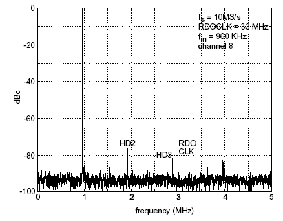
Figure 4. Effect of readout clock on closest ADC
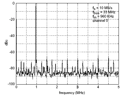
Figure 5. Effect of bus activity on closest ADC
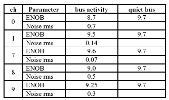
Table 3. ADC Performance with and without bus activity
5. Conclusions
Nowadays High-Energy Physics experiments demand the integration in a single chip of the ADC and the data processing logic for a high number of channels. The ALTRO chip, developed for the ALICE experiment at the CERN LHC, represents the first ASIC of these characteristics. The measurements show that it is possible to integrate a high number of ADCs together with a large amount of processing logic without affecting the performance of the standalone ADC. The key is to make a design that can tolerate noise, rather than trying to completely insulate noise.
6. References
[1] CERN/LHCC 95-71 LHCC/P3, A Large Ion Collider Experiment, ALICE-Technical proposal, Dec. 1995, ISBN 92-9083-077-8, Geneva, Switzerland
[2] A Large Ion Collider Experiment, ALICE TPC -Technical Design Report, Dec. 1999, ISBN 92-9083-155-3, Geneva, Switzerland.
[3] L. Musa et al., Front_End Electronics for the ALICE-TPC Detector, Proc. of the 4th Workshop on Electronics for LHC Experiments, Rome, Sept. 21-25, 1998.
[4] http://www.st.com/stonline/stdics/index.shtml
[5] T.B. Cho, P.R. Gray, “A 10b/20 Msamples/s 35mW pipeline A/D Converterâ€, IEEE JSSC, vol.30, no.3, 1995, pp.166-172.
[6] D. Cline, P. Gray, “A Power Optimized 13-b 5 Msamples/s Pipelined Analog-toDigital Converter in 1.2mm CMOSâ€, IEEE JSSC, vol.31, no.3, March 1996, pp. 443-452.
[7] K. Bult and A. Buchwald, “An embedded 240mW 10b 50- MS/s CMOS ADC in 1 mm2â€, IEEE JSSC, vol.32, Dec. 1997, pp. 1887-1895.
[8] B. Mota et al., Digital Implementation of a Tail Cancellation Filter for the Time Projection Chamber of the ALICE Experiment, Proc of the 6th Workshop on Electronics for LHC Experiments, Krakow, Sept. 11-15, 2000.
Related Semiconductor IP
- NPU IP Core for Mobile
- NPU IP Core for Edge
- Specialized Video Processing NPU IP
- HYPERBUS™ Memory Controller
- AV1 Video Encoder IP
Related White Papers
- BCD Technology: A Unified Approach to Analog, Digital, and Power Design
- Achieving Lower Power, Better Performance, And Optimized Wire Length In Advanced SoC Designs
- Context Based Clock Gating Technique For Low Power Designs of IoT Applications - A DesignWare IP Case Study
- eFPGAs Bring a 10X Advantage in Power and Cost
Latest White Papers
- Ramping Up Open-Source RISC-V Cores: Assessing the Energy Efficiency of Superscalar, Out-of-Order Execution
- Transition Fixes in 3nm Multi-Voltage SoC Design
- CXL Topology-Aware and Expander-Driven Prefetching: Unlocking SSD Performance
- Breaking the Memory Bandwidth Boundary. GDDR7 IP Design Challenges & Solutions
- Automating NoC Design to Tackle Rising SoC Complexity