BCD Technology: A Unified Approach to Analog, Digital, and Power Design
By Abhishek BV, eInfochips
Abstract:
Since its inception, BCD technology has leveraged the integration of two primary technologies—polysilicon gate CMOS and DMOS power architecture—on the same chip. Its compatibility with bipolar components has enabled the creation of SoCs (System-on-Chip) that combine digital and analog control with efficient power management sections. The BCD process generation was built from the CMOS baseline and the geometric scaling rules of the new lithography nodes to achieve overall reductions in area and cost for all integrated functions. Historically, the evolution of the BCD technology platform has been driven by key application segments such as hard disk drives for computing and motion control for industrial applications.
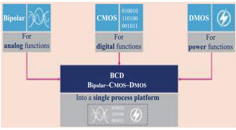
BCD (Bipolar CMOS DMOS) is a process used to drive high voltage components and is widely used in a variety of applications like audio amplifiers, RF (radio frequency), and automotive industry. It is a key technology for power ICs. This process involves bipolar for precise analog functions, CMOS for digital design, and DMOS for power and high voltage. It means a single chip carries three functions shown in figure 1.1. The three functional sections are designed with distinct development and optimization criteria.
However, their integration is crucial to achieving the correct system functionality. Each section independently cannot fulfill the system's intended purpose. They must work together synergistically to deliver the desired overall functionality. To achieve the best performance and minimize self-heating due to dissipation, it is important to position the different sections as close to each other as possible. This proximity reduces parasitic effects, minimizes signal delays, and enhances thermal management by allowing efficient heat dissipation across the chip as shown in figure 1.2.
BCD (Bipolar CMOS DMOS)
The typical BCD technology offers low voltage logic CMOS transistors, high voltage transistors, diodes, resistors, and MIM capacitors in the same process. The BCD process has parasitic bipolar transistors that are good to make analog circuits like band gap reference.

Figure 1.1

Figure 1.2
Advantages of using BCD technology:
- Improved system reliability
- Reduced Electromagnetic interference
- Smaller chip area
- High energy efficiency
BCD Technology Architecture

Figure 2.1
C- Collector, B- Base, E- Emitter S – Source, G – Gate, D – Drain, B – Bulk/Body
The above figure 2.1 shows the typical BCD technology architecture.

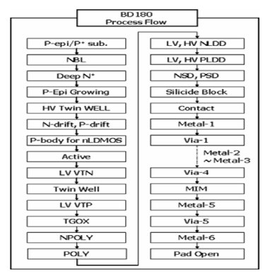
Figure 3.1 (reference: Il-Yong Park, Yong-Keon Choi, Kwang-Young Ko, Chul-Jin Yoon, Bon-Keun Jun, Mi-Young Kim, Hyon-Chol Lim, Nam-Joo Kim and Kwang-Dong Yoo Analog Business Division, Dongbu HiTek 222-1, Dodang-Dong, Wonmi-Gu, Bucheon, Gyeonggi-Do, 420-712 Korea)
The above figure 3.1 shows the BCD technology process flow.
BCD Process flow Overview:
- Start with Bulk Substrate:
- Thick silicon wafer.
- Heavily doped with p-type impurities.
- Epitaxial Deposition:
- A thin layer of slightly p-doped silicon grown on the substrate.
- Uses epitaxial (epi) deposition techniques.
- Purpose of the Epitaxial layer:
- Serves as the starting point for subsequent fabrication steps.
- Critical for semiconductor device manufacturing.
- Doping level considerations (Balancing Doping levels):
- Substrate Resistance:
- It should not be too low that avoids excessive electrical resistance in the substrate which could impair device performance.
- Substrate Resistance:
The crystalline structure of the silicon should not be too high, as it ensures good electrical properties and reliability of fabricated devices.
The process flow begins with the bulk substrate, which is a thick silicon wafer heavily doped with p-type impurities.
- When currents are injected into the substrate, having a small substrate resistance results in lower noise and higher electrical stability. This is because the parasitic bipolar transistors formed by the substrate and isolation rings are less likely to be triggered by higher currents.
- Maintaining a low substrate resistance helps in minimizing parasitic effects and improving the overall performance and reliability of semiconductor devices.
- Next, we implant the buried layer, a highly N-doped region created by implanting antimony (Sb) ions very superficially.
- After that a new P- type epitaxially layer grows above the buried layer to host the active areas.
- Then deep trench isolation is implemented to achieve lateral isolation between different sections of the die where performance and noise rejection are crucial. This technique involves etching deep trenches into the substrate and filling them with dielectric material such as silicon dioxide (SiO2).
- Deep trench isolation effectively isolates active regions of the semiconductor device from each other, reducing crosstalk, leakage currents, and other unwanted interactions that can degrade performance and increase noise. This isolation technique is particularly important in high-performance integrated circuits where precise control over electrical isolation is essential for optimal functionality.
- Later, active areas are defined for an integrated circuit. According to the technological node and specific design rules, the active area on a semiconductor wafer can be allocated for a single device or multiple devices. This allocation depends on various factors such as the desired circuit functionality, layout constraints, and the level of integration required for the design.
- In semiconductor design, it's vital to prevent current flow between different active areas. This is typically achieved through effective isolation techniques such as Locally Oxidizing Silicon (LOCOS) or adopting the Shallow Trench Isolation (STI).
- Next, we implant the wells that need the greatest thermal budget (HV well). Particularly, they are the isolation wells (isolated regions within the substrate that prevent electrical interaction between different parts of the circuit), the wells of the LD-MOSFET (n-well or p-well to optimize their performance and isolate them from other components on the chip), and the body of the high voltage n-MOS and p-MOS (isolated to ensure proper biasing and prevent unintended currents that could lead to device malfunction or breakdown).
- After implantation processes in semiconductor fabrication, the substrate undergoes a thermal annealing process in a furnace. This annealing step is essential to activate dopants implanted into the substrate and to repair any crystal damage caused during implantation.
- The annealing process typically involves heating the wafer to high temperatures in a controlled environment, allowing dopants to diffuse into the silicon lattice and form the desired electrical junctions. This thermal treatment also helps to relieve stress in the crystal structure, improving the overall quality and reliability of the fabricated semiconductor devices.
- We also implant the wells that need the lowest thermal budget (LV well). After implantation, the substrate undergoes the necessary thermal processing through Rapid Thermal Annealing (RTA).
In semiconductor manufacturing, the gate oxide of MOSFET transistors is grown using the In-Situ Steam Generation (ISSG) process. This method involves generating steam (H2O) in situ, typically through the reaction of hydrogen (H2) with oxygen (O2) on the wafer surface. The steam is then used to grow a thin layer of silicon dioxide (SiO2), which serves as the gate oxide.
For high-voltage devices, the gate oxide is initially grown to its maximum required thickness. Following this, a masking step is performed, where a mask is applied to define the areas where the oxide is needed. The exposed areas of the oxide are then etched away, leaving behind the gate oxide only in the desired regions. The gate oxide growth continues, with a focus on achieving the desired final thickness. This growth may partially extend into the high-voltage regions as needed, ensuring uniformity and proper insulation across the entire substrate. After doping a thick polysilicon layer, high doses of boron or arsenic are implanted into specific regions where n+ or p+ regions need to be created. A silicide layer is formed in specific areas where metal contact is made. The formation of a silicide layer effectively transforms the semiconductor-metal junction into a metal-metal junction. The last step is the Backend-of-Line (BEOL) process that refers to the final stages of fabrication involving the integration of metal interconnections.
Generally, MIM capacitors are used in BCD technology since they minimize the parasitic capacitance to the substrate. MIM capacitors are preferably implemented between the upper metal levels of the technology BEOL. Another advantage of MIM capacitors is that they can be stacked above active components, reducing the die size compared to other solutions.
Most commonly there are four terminals (Gate Source Drain Bulk) for PMOS/NMOS devices in CMOS but in our design, we had seven PMOS terminals and six NMOS terminals devices shown in figure 4.1 and figure 4.2 below, respectively.

Figure 4.1

Figure 4.2
The other three terminals in our devices were:
DPW (Deep P Well) - Deep P well shields the N well which contains the PMOS transistors, preventing it from collecting signal charge from the epitaxial layer instead of the N well as charge collection electrode.
ISO NBL (Isolated N type buried layer) – To achieve isolation between circuits operating at different voltages or to prevent noise coupling through a common P-substrate. It serves as a buried layer of N-type dopants within the P-substrate. This layer effectively isolates different regions of the substrate from each other, preventing unintended electrical interactions and reducing noise propagation between circuits. ISO NBL helps in minimizing noise coupling through the substrate.
SUB ISO (Isolated Substrate) – Large number of switching in the digital blocks may impact the performance of the RF and analog blocks and vice versa. We can isolate various blocks of the circuit from each other so there is least coupling between the RF and digital blocks through the substrate. Of course, there are interactions between power and ground lines, which have to be addressed in their own right.
This isolation allows HVNW (High voltage N-well) and NBL (N buried layer) to be in different potential.
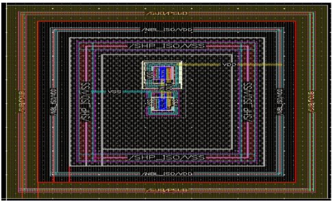
The DPW terminal is connected to the ground line, NBL terminal to the power line, and SUB terminal is connected to the ground line.
The layer information of the ISO ring is shown in figure 5.1.
All the clusters of PMOS and NMOS devices were placed in an Isolation ring shown in figure 5.2 below.

Figure 5.1

Figure 5.2
To handle high-voltage signals with typical MOS (Metal-Oxide-Semiconductor) devices, device terminals are often floated allowing flexibility in handling high-voltage signals while maintaining operational integrity and protecting against electrical stress. In CMOS (Complementary Metal-Oxide-Semiconductor) processes, substrate floating can indeed degrade performance, primarily due to the low resistivity of the substrate.
To address the challenges associated with substrate floating and improve performance in CMOS designs, the triple well structure is employed. This structure effectively isolates the body of the transistor and the deep N well from the substrate, enabling separate biasing. Isolation effectiveness can vary with frequency due to parasitic capacitances and other factors. At low frequencies, isolation is generally effective because the off-state resistance between isolated regions, such as between the deep N well and the substrate, is high. This high resistance minimizes leakage currents and prevents direct coupling of signals between different regions.
References:
G. Croce, A. Andreini, P. Galbiati
(STMicroelectronics, Department of Smart Power R&D, Agrate Brianza (MI), Italy)
C. Diazzi
(STMicroelectronics, Department of Smart Power Technology, Cornaredo (MI), Italy)
Danilo Covello (POLITECNICO DI TORINO)
Author: Abhishek BV

Author Bio: Working as a Senior Engineer in eInfochips for over two years and having overall 6+ years of experience in Analog layout design. Graduated in Electronics & Communication engineering.
Related Semiconductor IP
- NPU IP Core for Mobile
- NPU IP Core for Edge
- Specialized Video Processing NPU IP
- HYPERBUS™ Memory Controller
- AV1 Video Encoder IP
Related White Papers
- A Heuristic Approach to Fix Design Rule Check (DRC) Violations in ASIC Designs @7nm FinFET Technology
- Agile Analog's Approach to Analog IP Design and Quality --- Why "Silicon Proven" is NOT What You Think
- It's Just a Jump to the Left, Right? Shift Left in IC Design Enablement
- How to Elevate RRAM and MRAM Design Experience to the Next Level
Latest White Papers
- Transition Fixes in 3nm Multi-Voltage SoC Design
- CXL Topology-Aware and Expander-Driven Prefetching: Unlocking SSD Performance
- Breaking the Memory Bandwidth Boundary. GDDR7 IP Design Challenges & Solutions
- Automating NoC Design to Tackle Rising SoC Complexity
- Memory Prefetching Evaluation of Scientific Applications on a Modern HPC Arm-Based Processor