COMSIS 802.11n: an IP to Reuse - a flexible platform for Design
By Roxana Ojeda and Philippe Leclair, Comsis
Abstract:
Comsis, a fabless company, designs WiFi technologies. In 2003 when MIMO (Multiple Inputs / Multiple Outputs) recommendation did not exist, we developed and exhibited at CES a proprietary 2x2 MIMO WiFi solution based on Golden code at a rate of 24 Mbps for multimedia applications. A demonstrator had been designed around this IP using a Commercial Altera motherboard where the baseband module was programmed and two externally synchronised MAX2829 Maxim evaluation boards were used as RF board. Some additional daughter cards were designed by COMSIS to increase the number of codecs of two to four that is necessary for a 2x2 I/Q implementation. In February 2007, with 802.11n Draft 2.0 approval, COMSIS decided to develop this IP taking advantage of our skill in this topic as well as a 3x3 MIMO baseband/dual band RF platform. In 2008, this kit became available allowing the design, test and validation of WiFi circuits.
For consumer applications, a system on chip (SoC) provides the best economical choice. This is the current roadmap step of Comsis. Recently, a first SoC evaluation has proved the technical feasibility providing useful figures in term of size and speed which are crucial in the choice of functionalities of the final circuit.
In this paper, we present 802.11n Comsis IP and the Comsis WiFi evaluation board. First, we summarize 802.11n recommendation features explaining why the MIMO technology performs so well.
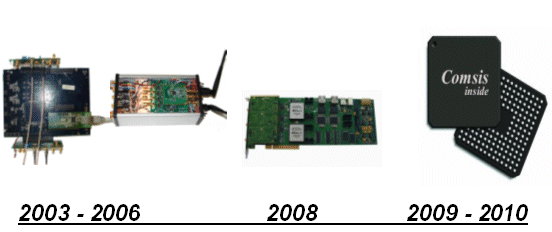
Figure 1: COMSIS roadmap design
ADVANTAGES OF WIFI MIMO SCHEME
In a few years, wired services will be completely replaced by the wireless system. Among them, the mobile telephone application is the main current wireless service but it does not cover requirements of future applications such as Internet and multimedia that need a higher rate. Further, it is very expensive because the user must pay for each service. Using a WiFi solution, the user becomes owner of his network that can be deployed with a low infra structure cost (unlicensed spectrum, cheaper resources). The implementation of the MIMO technology with spatial diversity leads better performances including a higher data rate than the classical WiFi SISO (Single Input/Single Output) system, for the same radiated power and bandwidth. A MIMO transmitter is based on a coder that splits the binary information in several independent streams allowing the increase of the data rate. Besides, with several antennae at the receiver, the probability to recover a non-fading signal is higher and as a consequence, the system performances are improved.
802.11N COMSIS IP DESCRIPTION
The 802.11n recommendation is the new generation WiFi system based on the existing 802.11a/b/g WiFi that includes a package of technologies, specially the MIMO physical layer technique that enhances the communication link quality.
We focalise on the mandatory features included in our implementation that supports up to 2 spatial streams and operates in 2.4 GHz or 5 GHz with 20 MHz of bandwidth. Two transmission modes are provided: the Legacy Mode inherited of 802.11a/g systems (with 8 sub-modes) and the Mixed Mode which provides 16 new rates. The latter format frame contains the legacy compatible preamble and high throughput (HT) training symbols and parameters (rate, bandwidth, length).
A general transmission diagram is depicted in figure 2. The violet blocks represent new or modified functionalities with respect to 802.11a/g. These features provide a best performance of the system given by the spatial and temporal diversity strategies included (parser, two different interleavers, cyclic shift, pilots mapping and two antennae). The system operates with 64-points OFDM modulation (IFFT/FFT blocks) where
there are 4 frequencies that are pilot subcarriers and 48 or 52 others are data subcarriers for legacy and HT modes respectively. As a consequence, in HT mode, the four additional data subcarriers and a 5/6 rate puncturer increase the supported data rate up to 130 Mbps.
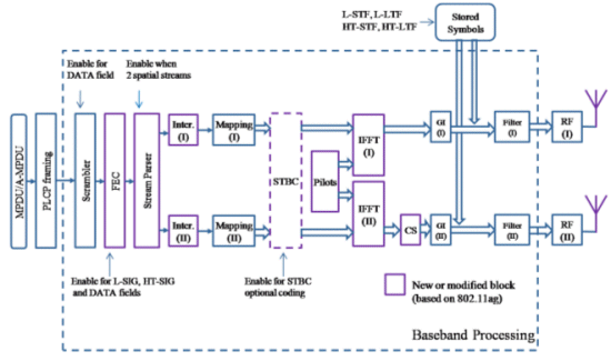
Figure 2: Transmitter scheme
Figure 3 shows Comsis 802.11n IP receiver architecture where two kinds of sensitive tasks have been remarked: signal processing and MIMO decoder blocks. Signal processing tasks can be observed in dark blue blocks. They consist of the automatic gain control algorithm, the frame detection and synchronisation task and the initial frequency offset estimation and compensation plus the tracking operation all along the frame. These
functionalities that are hardware dependent can be configured taking into account noise and signal levels as well as the speed of analog components.
The Comsis Mimokit platform configuration is included by default in the Comsis 802.11n IP.
The light blue block of figure 3 depicts the MIMO decoder. It is the key of our technology in terms of transceiver performances and hardware complexity points of view. As it knows, recommendations propose the technology to apply but a smart implementation relies on the skills of the designer. Further, for a given algorithm, the best performance, ideally near the theoretical limits, is reached at the expense of a strong hardware complexity. Of course, the goal is to obtain a fair compromise between these two opposite requirements.
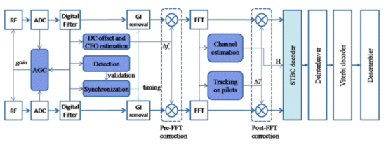
Figure 3: Receiver scheme
As next step, COMSIS foresees to develop some options of the 802.11n recommendation with the goal to increase the data rate. One of these options is the 40 MHz mode. Using the twice of mandatory bandwidth mode and the same numerical modulations, a maximum rate of 270 Mbps can be provided. A quick implementation of this circuit can be achieved increasing the processing clock speed of twice and reusing the 20 MHz mode hardware architecture.
Another possibility to increase throughput that simultaneously improves performances is the implementation of more than two antennae in the transmitter and the receiver sides. In this case, a suboptimal design composed of several 2x2 circuits can provide a suitable WiFi transceiver regarding performances and cost.
Moreover, an enhanced 2x2 MIMO technology based on the Comsis Golden Code proprietary scheme and compliant with 802.11n recommendation is included in Comsis product catalogue. This circuit performs better than a 2x3 MIMO 802.11n standard solution with a lower hardware cost.
COMSIS MIMO WIFI PLATFORM DESIGN
Figure 4 illustrates Comsis WiFi platform. This kit has been conceived to facilitate the design and the validation of new baseband or WiFi products to be implemented in FPGA or Asic technologies as well as to develop applications around Comsis 802.11n IP. This platform can also be useful as commercial demonstrator of products. It is composed of two independent boards: the motherboard where the baseband can be implemented and a 3x3 2.4GHz/5GHz RF daughterboard. The radio card design is based on the SISO dual-band MAX2829 Maxim component. As a MIMO transceiver requires the same master frequency for all streams, a local oscillator of 40 MHz is shared for the three radio components.
Two large FPGAs (Altera Stratix II) components are included in the motherboard. The FPGA1 component has pins directly routed towards the analog front-end (AFE) circuit and the RF board. The FPGA2 component is connected to several peripheral interfaces (2 Giga Ethernet, 2 USB2s, 1 PCI bus, 2 RS-232s) and SDRAM and Flash memories. The two FPGAs are interconnected by a high speed bus. This architecture suggests the partition of tasks between the two FPGAs: the physical layer is programmed in the FPGA1 and the
MAC and higher layers functionalities are fitted in the FPGA2. Regarding our 802.11n IP solution, an half of the FPGA1 and a third of the FPGA2 are used.
Others components are available as part of the kit: two oscillators of 40MHz and 66MHz, a JTAG connector needed to program and debug designs, flash memories allowing the download of codes into the FPGAs at boot.
A universal high speed SAMTEC connector permits plugging the chosen WiFi RF target board or a RF daughter card for any other wireless application. For a whole baseband prototype, COMSIS provides a three I/O SMA connectors baseband interface card to plug in the SAMTEC expansion connector.
The AFE module is made of three AD9861 Analog Devices dual codecs. Each codec contains two matched 10-bit DACs and two matched 10-bit ADCs typically operating at 80 MHz. These components can be configured by using pins or SPI protocol and programmed in several modes. For each dual codec two I/Q streams in half duplex mode (non-simultaneous transmission/reception) must be implemented during WiFi link. On the other hand, during the initial RF calibration process, all flows are set in full duplex mode.
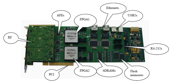
Figure 4: MIMOkit FPGA development platform
AN 802.11N LOW LEVEL VHDL CODE
The Comsis 802.11n IP has been implemented in a technology-independent VHDL code leading to reduce the time-to-market for a SoC.
However, an appropriate set of synthesis options will directly provide macro-cells instantiations (particularly memories and DSPs) and consequently a better resources sharing when the target is a FPGA. The synthesis summary of an 802.11n physical layer given by the Quartus II tool is illustrated in the following table. The synthesis is realized on the Altera Stratix II EP2S180F1020C using DSPs, PLLs and memories macro-functions and the speed optimisation option to achieve a processing clock of 80 MHz.
Comsis 802.11n physical layer code includes serial and parallel PHY/MAC interfaces as well as RF and AFE controllers that simplify the implementation of code in the chosen hardware by using a high level configuration application.
Further, this code has been written taking into account VHDL design rules that have been checked with LEDA tool.
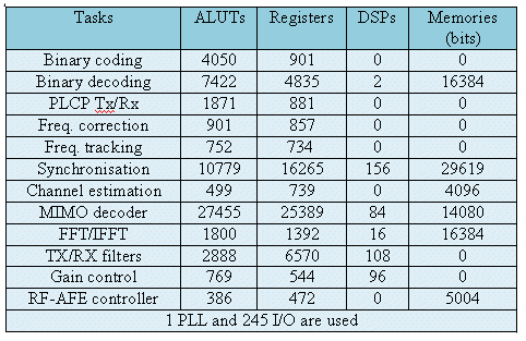
Figure 5: Resource utilisation by entity
In spite of the intensive optimisation effort spent in this design, figure 5 shows that hardware complexity of 802.11n transceiver is brought about two tasks of the receiver side: the MIMO decoder and the synchronisation. Further, some tasks as the Viterbi algorithm of the binary decoder and the OFDM modules (FFT/IFFT) where data is processed by block employ strong memory resources. For the same raison, several registers are required by the interleaver/deinterleaver modules of the binary coding/decoding. A large number of registers and DSPs are needed to simultaneous implementation of multiplications and additions on N-depth samples vectors defined in the TX/RX filter tasks.
The software MAC layer and the applications run in a microcontroller programmed in the FPGA2. This processor has been designed for this specific application from the standard VHDL code of Gaisler LEON3 microcontroller. Taking into account no critical requirements in term of processing effort and speed, i.e. 320 MHz, cost and flexibility are the criteria that have been considered in the choice of this microcontroller.
To complete the design, a MAC layer and several standard interfaces IPs have been used.
The Comsis 802.11n architecture associated to the designed Comsis MIMOkit follows the structure of the first version of 802.11n Comsis SoC illustrated in figure 6. The goal of this approach is to sure the functional and technological correctness of the SoC by early tests and validations for similar constraints.
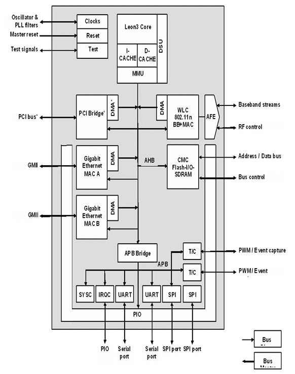
Figure 6: Comsis 802.11n SoC architecture
CRITICAL DESIGN POINTS
In this paragraph, details regarding critical points found during the RF board design and the motherboard integration are described as well as the implementation of hardware or software solutions.
Moreover, some key points of automatic gain control algorithm are discussed.
The MIMO scheme requires that all transceivers share the same local oscillator in order to guarantee the frequency coherence. In the RF board, a unique oscillator is used as the clock reference. This component is followed by a precise buffer tree where each branch feeds one transceiver MAX2829. For our first RF design, the buffer had altered the clock signal provoking a phase noise distortion because the transition levels at the output of buffer slightly varied from cycle to cycle. Hence, a new circuit has been designed by removing the buffer and by taking care of routing constraints of the clock signals.
Another distortion has been produced by the mismatch of resistances which fix the ADCs common mode. As a consequence, an offset signal is generated between the differential inputs of this component. This perturbation that is temperature- sensitive has been compensated by a digital filter implemented in FPGA data inputs. The 802.11n OFDM spectrum does not send information in zero frequency but the spectre includes a lower data subcarrier at 300 KHz. In this task, it is important to pay particularly attention to the quality of the filtering operation to avoid a spectral distortion.
The automatic gain control (AGC) is an adaptive algorithm found in several electronic devices that provides a approximately constant average level of the signal. The AGC algorithm calculates the gains to provide at the RF board based on the estimated signal level. This algorithm that is heavily depending on the hardware demands a precise model of it. Parameters such as noise figure, reaction times, and sensibility must be well known, sometimes recovered by experiences, to fix a large amount of parameters and thresholds of the algorithm.
PROSPECTS AND APPLICATIONS
The WiFi is now a worldwide well known deployed wireless system. After genesis of first standards a/b/g mainly dedicated to internet applications, ,the time of its maturity came with ‘n’ and new deal such as QoS (Quality of Service) and applications such as VoIP, HiFi, video and sustainable development.
Next applications including WiFi will also take place in automotive domain. For example, the IEEE 802.11p recommendation is an adaptation of IEEE 802.11n one, in 5 MHz bandwidth.
Regarding the communication between two cars or a car and a base station, a WiFi link seems an interesting choice because it can be deployed using the growing WiFi infrastructure and installing a WiFi transceiver into the cars. Using real time traffic information, the goal of this application is to regulate the traffic flow by an automatic action on the speed of the cars, in situations such as high traffic density or incidents and also to provide instantaneous navigation information downloaded in live. As a consequence of the radio propagation in a high-speed mobile environment, the Doppler Effect appears and an estimation and compensation of this phenomenon must be implemented. The 802.11n recommendation has not been designed to cover these aspects but the new recommendation 802.11p takes into account the processing of this distortion.
Enhancements of MAC used in conjunction of PHY supporting MIMO address these new challenges. Indeed, 802.11n recommendation improves the QoS of multimedia applications but it damages the quality of data service. The equity amongst different services can be expected by reducing the number of packet collisions. Therefore exchanges will be more efficient and the available channel time will be increased.
For economical and public-health reasons, a true effort must take place to decrease the power consumed by WiFi devices. Regarding the design of low power products, several aspects must be considered to reduce the power consumption. In a theoretical domain, it will be interesting to include the power as a constraint on the algorithm design. At the implementation level, an appropriated circuit architecture based on protocol interfaces that efficiently manage power must be considered. Regarding integration level, the power consumption required depends on the SoC technological target. Finally, at the application level, the software can save power by turning off equipments during idle times.
CONCLUSIONS
This paper presents an overview of main features of Comsis 802.11n IP and Comsis MIMOkit based on FPGA in terms of performances, flexibility and hardware architecture.
Regarding a theoretical point of view, we discussed the benefit provided by the MIMO technologies.
In a technical point of view, we have shown the qualities of Comsis 802.11n IP to be implemented and reused on different technological targets with a minimum of time-to-market.
We have shown the versatility of Comsis 802.11n MIMOkit to develop new applications around Comsis 802.11n IP or in the design of new wireless or baseband products.
Moreover, the Comsis 802.11n IP or a modified version and the Comsis 802.11n MIMOkit is the ideal couple to test and validate preliminarily a SoC circuit.
Finally, implementation proposals about different options of IEEE 802.11n recommendation, and the modifications of this standard for a better QoS have been discussed in this paper. These modifications concerning future applications take into account a more realistic channel propagation model and the global optimisation of traffic for different classes of services.
Related Semiconductor IP
- Ultra low power 2.4GHz 802.11n + PA + RFSW
- IEEE 802.11n RF/Baseband/MAC 40nm
- IEEE 802.11n/ac/ax (WiFi) LDPC Decoder and Encoder
- IEEE 802.11n/ac/ax Encoder and Decoder
Related White Papers
- CSoC Platform / Digital Subsystem IP for IoT
- One Platform, Five Libraries: Certus Semiconductor’s I/O IP Portfolio for Every Application on TSMC 22nm ULL/ULP Technologies
- Creating IP level test cases which can be reused at SoC level
- Pondering the SoC platform
Latest White Papers
- Ramping Up Open-Source RISC-V Cores: Assessing the Energy Efficiency of Superscalar, Out-of-Order Execution
- Transition Fixes in 3nm Multi-Voltage SoC Design
- CXL Topology-Aware and Expander-Driven Prefetching: Unlocking SSD Performance
- Breaking the Memory Bandwidth Boundary. GDDR7 IP Design Challenges & Solutions
- Automating NoC Design to Tackle Rising SoC Complexity