Faraday Accelerates AI Revolution with Its FPGA-to-ASIC Conversion Service
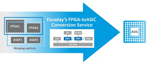
Hsinchu, Taiwan Mar. 12, 2018 -- Faraday Technology Corporation (TWSE: 3035), a leading ASIC design service and IP provider, today announced its FPGA-to-ASIC conversion service has successfully completed several AI related projects including drone vision, medical image analysis, smart appliances, and 3D sensing. It brings remarkable power saving, enhanced performance and lower system cost to meet the specific AI requirement.
Faraday’s FPGA-to-ASIC conversion service, in conjunction with comprehensive IP solutions of PCIe Gen 3/4, MIPI D-PHY, DDR3/4 and SerDes 12/16/25/28/56G at advance FinFET process nodes, are particularly suited for AI chips requiring higher bandwidth and a lower latency interface. From cloud to edge computing, in applications like machine vision, NLP, and sentiment analysis, Faraday can deliver optimized ASIC chip designs featuring 30~100 times better energy efficiency.
With 25 years of IP development experience, Faraday has the ability to customize IPs for ASIC cost efficiency in mass production. Faraday has handcrafted SRAM macros allowing for a reduction of on-chip SRAM area by 5~50%, in addition, its SRAM Redundancy & Repair design feature increases yield rates by up to 10%.
“As AI algorithm mature and the market demand for AI products rise, customers look to replace FPGA chips with ASIC devices for a competitive system BOM cost. Faraday’s ASIC service has been validated in thousands of designs and shipped hundred millions of market proven SoCs. The service provides AI customers with a path to lower integration risk and cost, accelerating the adoption of new DNN algorithms”, said Flash Lin, COO of Faraday Technology.
About Faraday Technology Corporation
Faraday Technology Corporation (TWSE: 3035) is a leading ASIC design service and IP provider, certified to ISO 9001 and ISO 26262. The broad silicon IP portfolio includes I/O, Cell Library, Memory Compiler, ARM-compliant CPUs, DDR2/3/4, low-power DDR1/2/3, MIPI, V-by-One, USB 2.0/3.1 Gen 1, 10/100/1000 Ethernet, Serial ATA, PCI Express, and programmable SerDes, etc. Headquartered in Taiwan, Faraday has service and support offices around the world, including the U.S., Japan, Europe, and China. For more information, please visit:www.faraday-tech.com
Related Semiconductor IP
- 6-bit, 12 GSPS Flash ADC - GlobalFoundries 22nm
- LunaNet AFS LDPC Encoder and Decoder IP Core
- ReRAM NVM in DB HiTek 130nm BCD
- UFS 5.0 Host Controller IP
- PDM Receiver/PDM-to-PCM Converter
Related News
- Faraday Unveiled FPGA-Go-ASIC Prototyping Platform to Accelerate FPGA-to-ASIC Conversion
- Faraday Exhibits AI FPGA-to-ASIC Solution and IoT SoC Platform at DAC 2018
- Faraday ASIC Service Leverages Samsung FinFET Platform to Target Next-generation Applications
- Faraday Delivers System-Level ESD Protection Service to Reduce ASIC Time-to-Market
Latest News
- Seligman Ventures Leads Cognichip’s $60M Series A to Back Physics-Informed AI for Chip Design, Intel CEO Lip-Bu Tan and Seligman Ventures’ Umesh Padval Join the Board
- SEMI Projects Double-Digit Growth in Global 300mm Fab Equipment Spending for 2026 and 2027
- Intel to Repurchase 49% Equity Interest in Ireland Fab Joint Venture
- AGI CPU: Arm’s $100B AI Silicon Tightrope Walk Without Undermining Its Licensees
- EnSilica selected for UK CHERI Adoption Collective