Faraday Exhibits AI FPGA-to-ASIC Solution and IoT SoC Platform at DAC 2018
HSINCHU, Taiwan -- June 12, 2018 -- Faraday Technology Corporation (TWSE: 3035), a leading ASIC design service and IP provider, today announced that it will showcase their AI FPGA-to-ASIC solution and the Uranus+™ ultra-low-power IoT SoC development platform at Design Automation Conference (DAC), June 25-27, 2018 in San Francisco, CA, USA.
Faraday’s FPGA-to-ASIC conversion service has successfully completed several AI related projects including drone vision, medical image analysis, smart appliances, and 3D sensing. It brings remarkable power savings, enhanced performance, and lower system cost to meet specific AI requirements. By leveraging a comprehensive IP solutions suite and advanced FinFET process nodes, the service is particularly well suited for AI chips requiring higher bandwidth and a lower latency interface.
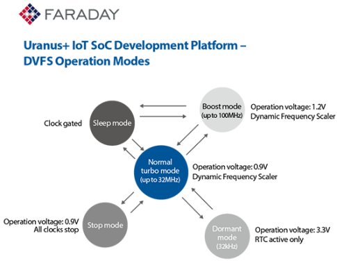
The demonstrated Uranus+ platform is a 32-bit MCU-based ultra-low-power SoC with embedded flash, implemented by UMC 55ULP technology, targeting to accelerate the development of IoT applications. It features DVFS power modes management to balance trade-offs between performance and power consumption. In particular, its Turbo Mode enables MCU core to achieve 2x performance under same operating voltage.
"We are very excited to present our latest ASIC solutions at DAC," said Flash Lin, Chief Operating Officer of Faraday. "Founded since 1993, we position ourselves as the driver of ASIC design service innovation. As the demand for AI ASIC chips is growing, we look forward to exploring more opportunities at the show and building strong business relationships in the US."
Visit Faraday’s booth at #2138 and find out the latest solutions from Faraday.
About Faraday Technology Corporation
Faraday Technology Corporation (TWSE: 3035) is a leading ASIC design service and IP provider, certified to ISO 9001 and ISO 26262. The broad silicon IP portfolio includes I/O, Cell Library, Memory Compiler, ARM-compliant CPUs, DDR2/3/4, low-power DDR1/2/3, MIPI, V-by-One, USB 2.0/3.1 Gen 1, 10/100/1000 Ethernet, Serial ATA, PCI Express, and programmable SerDes, etc. Headquartered in Taiwan, Faraday has service and support offices around the world, including the U.S., Japan, Europe, and China. For more information, visit www.faraday-tech.com.
Related Semiconductor IP
- UCIe D2D Adapter & PHY Integrated IP
- Low Dropout (LDO) Regulator
- 16-Bit xSPI PSRAM PHY
- MIPI CSI-2 CSE2 Security Module
- ASIL B Compliant MIPI CSI-2 CSE2 Security Module
Related News
- Faraday Unveils FlashKit™-22RRAM: an eNVM-based SoC Development Platform for IoT
- Faraday Adds QuickLogic eFPGA to FlashKit‑22RRAM SoC for IoT Edge
- Faraday Reports 2018 Annual Revenues of NT$4.91 Billion, NRE NT$1.3 Billion, up 107% YoY; 2018 Gross Margin was 53.1%, a 11 Year High
- Faraday Showcases FinFET ASIC Solutions and SoCreative!V SoC Platform at DAC 2019
Latest News
- Wind River Joins the CHERI Alliance and Collaborates with Innovate UK to Accelerate Cybersecurity Innovation
- Arteris and MIPS Partner to Accelerate Development for Physical AI Platforms
- DCD-SEMI expands CryptOne with EdDSA Curve25519 IP core for secure embedded systems
- Syntacore's SCR RISC-V IP Now Supports Zephyr 4.3
- Xylon Presents New 12-Channel GMSL3/GMSL2 FMC+ ExpansionBoard