eSilicon Announces Availability of 7nm High-Bandwidth Interconnect (HBI+) PHY for Die-to-Die Interconnects
The PHY supports 2.5D applications such as silicon interposers and silicon bridges for system-on-chip (SoC) to chiplets and SoC partitioning
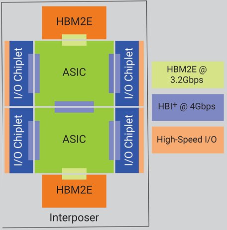
SAN JOSE, Calif. -- Sept. 22, 2019 -- eSilicon, a leading provider of FinFET ASICs, market-specific IP platforms and advanced 2.5D packaging solutions, announced today its 7nm high-bandwidth interconnect (HBI™)+ physical interface (PHY) IP is available to be licensed for inclusion in customer designs. This special-purpose hard IP block delivers a high-bandwidth, low-power and low-latency wide-parallel, clock-forwarded PHY interface for 2.5D applications including system-on-chip (SoC) to chiplets and SoC partitioning for complex subsystems. Silicon interposer and silicon bridge technologies are supported.
eSilicon’s HBI+ PHY delivers a data rate of up to 4.0Gbps per pin. Flexible configurations include up to 80 receive and 80 transmit connections per channel and up to 24 channels per PHY with one redundant lane per channel to improve production yields. The part also supports built-in self-test (BIST), internal loopback and external PHY-to-PHY link tests. Standards supported include IEEE 1149.1 (JTAG) and 1149.6 (AC JTAG) boundary scan.
“eSilicon has a rich history of developing high-performance, high-bandwidth interconnect IP, from long-reach SerDes to die-to-die interconnect,” said Hugh Durdan, vice president, strategy and products at eSilicon. “This new HBI+ PHY will help to enable a growing chiplet ecosystem that is supported by many new and innovative technologies.”
The prior version of this PHY (HBI, 2.5 Gbps per pin) was used successfully on a customer ASIC at 14nm. eSilicon is currently in design with a major customer ASIC in 7nm using the HBI+ PHY.
To learn more about eSilicon’s 7nm and 5nm HBI+ PHY capabilities, you can visit its HBI web page or contact your eSilicon sales representative directly or via sales@esilicon.com.
About eSilicon
eSilicon provides complex FinFET ASICs, market-specific IP platforms and advanced 2.5D packaging solutions. Our ASIC-proven, differentiating IP includes highly configurable 7nm 56G/112G SerDes plus networking-optimized 16/14/7nm FinFET IP platforms featuring HBM2 PHY, TCAM, specialized memory compilers and I/O libraries. Our neuASIC platform provides AI-specific IP and a modular design methodology to create adaptable, highly efficient AI ASICs. eSilicon serves the high-bandwidth networking, high-performance computing, AI and 5G infrastructure markets. www.esilicon.com
Related Semiconductor IP
- LPDDR5X/5/4X/4 combo PHY at 7nm
- 4.3GHz SSCG PLL on TSMC 7nm
- 12-bit 400MSPS ADC on TSMC 7nm
- Low Dropout (LDO) Capless Regulator on TSMC 7nm FFC
- Ultra‐Low‐Power Process/Voltage/Temperature Monitor on TSMC 7nm FFC
Related News
- eSilicon, Northwest Logic and SK Hynix create high-bandwidth memory (HBM) hardware demonstration
- High-performance, high-bandwidth IP platform for Samsung 14LPP process technology
- eSilicon announces 7nm FinFET ASIC design win
- 7nm networking platform delivers unprecedented performance and configurability for data center ASICs
Latest News
- Analog Bits Demonstrates Real-Time On-Chip Power Sensing and Delivery on TSMC N2P Process at TSMC 2026 Technology Symposiums
- TES offers a High-Frequency Synthesizer and Clock Generator IP for X-FAB XT018 - 0.18µm BCD-on-SOI technology
- Faraday Delivers IP Solutions to Enable Endpoint AI Based on UMC’s 28nm SST eFlash
- AiM Future Partners with Metsakuur Company to Commercialize NPU-Integrated Hardware
- ESD Alliance Reports Electronic System Design Industry Posts $5.5 Billion in Revenue in Q4 2025