PCIe Gen 2 IP
Filter
Compare
35
IP
from
15
vendors
(1
-
10)
-
PCIe Gen 2 Verification IP
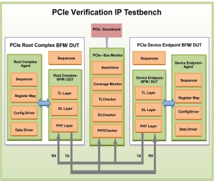
- Compliant with PCI Express Specifications 2.0 (5GT/s) and 1.1 (2.5GT/s).
- Verification IP configurable as PCI express Root Complex and Device Endpoint.
- Configurable LinkWidth: x1, x2, x4, x8, x12, x16, x32.
- Configurable pipe width : 8,16,32,64
-
AXI PCI Express (PCIe) Gen 3
- Maximum Payload Size (MPS) up to 256 Bytes
- Messaged Signaled Interrupt (MSI)
- Memory mapped AXI4 access to PCIe space
- PCIe access to memory mapped AXI4 space
-
PCIe Gen 7 Verification IP
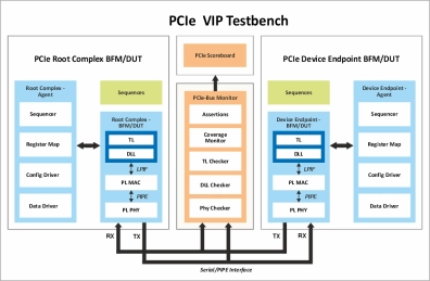
- The PCIe Gen 7 Verification IP provides an effective & efficient way to verify the components interfacing with PCIe Gen 7 interface of an IP or SoC.
- The PCIe Gen 7 VIP is fully compliant with latest PCI Express Gen 7 specifications. This VIP is a light weight with an easy plug-and-play interface so that there is no hit on the design cycle time.
-
PCIe Gen 6 Verification IP
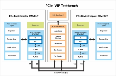
- Compliant with PCI Express Specifications 6.1 (64GT/s), 5.0 (32GT/s), 4.0 (16GT/s), 3.1 (8GT/s), 2.0 (5GT/s) and 1.1 (2.5GT/s).
- Support for 64.0 GT/s Data Rate per lane with backwards compatible.
- Support for new PAM4 Signalling and Gray Coding.
- Support for both Flit Mode & Non-Flit Mode.
-
PCIe Gen 5 Verification IP
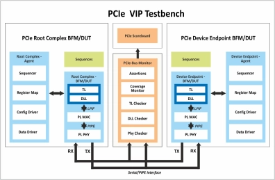
- Support for 32.0 GT/s Data Rate per lane with backwards compatible.
- Optimizing the Link to skip equalization at lower Data Rates when supporting 32.0 GT/s(optional feature).
- Lower pin count in pipe interface when supporting 32.0 GT/s.
- Support for newly added phy serdes architecture in pipe specification 5.0 .
-
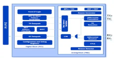
PCIe 2.0 Serdes PHY IP, Silicon Proven in SMIC 28HKMG
- Compatible with PCIe base Specification
- Full compatible with PIPE4.2 interface specification
- Independent channel power down control
- Implemented Receiver equalization Adaptive-CTLE to compensate insertion loss
-
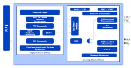
PCIe 2.0 Serdes PHY IP, Silicon Proven in SMIC 55LL/SP/EF
- Compatible with PCIe base Specification
- Full compatible with PIPE4.2 interface specification
- Independent channel power down control
- Implemented Receiver equalization Adaptive-CTLE to compensate insertion loss
-
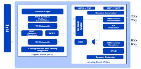
PCIe 2.0 Serdes PHY IP, Silicon Proven in SMIC 40LL
- Compatible with PCIe base Specification
- Full compatible with PIPE4.2 interface specification
- Independent channel power down control
- Implemented Receiver equalization Adaptive-CTLE to compensate insertion loss
-
PCI Express Gen 4 PHY
- Support 16GT 8GT 5GT 2.5GT data rate
- Compliant with PCI Express 4.0, 3.1, 2.1, 1.1 and PIPE 4.2 standards
- x1, x2, x4, x8, x16 lane configuration with bifurcation
- Multi-tap adaptive programmable continuous time linear equalizer (CTLE) and decision feedback equalizer (DFE)
-
PCIe 3.0 Serdes PHY IP, Silicon Proven in GF 22FDX
- Silicon Proven in GF 22GDX with 0.8V and 1.8V power supply.
- Compatible with PCIe base Specification
- Support 32-bit/16-bit parallel interface
- Support for PCIe3(8.0Gbps)
