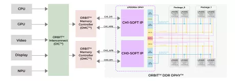
LPDDR4 Super Combo Interface IP
Filter
Compare
135
IP
from
16
vendors
(1
-
10)
-
DDR4 & LPDDR4 COMBO IO for memory controller PHY, 3200Mbps on TSMC 22nm
- The DDR4&LPDDR4 COMBO IO is used to transfer the Command/Address/Clk and Data between the memory controller PHY and the DRAM device
- The TX is designed to send information from PHY to DRAM and RX is designed to receive information which is from DRAM.
-
DDR4/ LPDDR4/ DDR3L PHY IP - 3200Mbps (Silicon Proven in TSMC 12FFC)
- Supported DRAM type: DDR3L/DDR4/LPDDR4
- Maximum controller clock frequency of 400MHz resulting in maximum DRAM data rate of 1866Mbps
- Interface: SSTL135/POD12/LVSTL
- Data path width scales in 32-bit increment

-
DDR4/ LPDDR4/ DDR3L PHY IP - 1866Mbps (Silicon Proven in TSMC 28HPC+)
- Supported DRAM type: DDR3L/DDR4/LPDDR4
- Maximum controller clock frequency of 400MHz resulting in maximum DRAM data rate of 1866Mbps
- Interface: SSTL135/POD12/LVSTL
- Data path width scales in 32-bit increment

-
DDR and LPDDR Combo PHY
- Supports multiple combinations of DDR/LPDDR interfaces
- Compliant with JEDEC DDR and LPDDR standards
- Supports all auto calibrations
- Industry leading area and power
-
LPDDR4X/4 & LPDDR5T/5X/5 Combo Controller
- Support for all LPDDR4 and LPDDR5 devices
- Bank management logic monitors status of each bank
-
LPDDR5X/5/4X/4 combo PHY at 7nm
- Compliant with JEDEC JESD209-5B for LPDDR5X/5/4X/4 with PHY standards
- Delivering up to 8533Mbps
- DFI 5.1 specification PHY Interface Compliant
- Support up to 4 ranks
-
I/O Library
- Supports process nodes from 0.13um to 3nm
- ESD protection: Robust ESD protection mechanisms ensuring device reliability and longevity
- Temperature Range: Designed for wide operational temperature ranges, suitable for consumer, AI to automotive applications
- Signal Integrity: Optimized for low noise and high signal integrity, ensuring reliable data transmission across all interfaces
-
Automotive IP Suite
- Our silicon proven Automotive IP Suite offers versatile and robust IP solutions for high-speed data communication in automotive applications.
- By supporting a wide range of industry standards, it provides automotive manufacturers with the flexibility and reliability needed to develop advanced, high-performance vehicle systems.
-
DDR4/LPDDR4 PHY Interface
- The DDR PHY IP is a combination of hard macro, I/O Pad and synthesizable RTL to provide a physical interface to JEDEC standard DDR3/DDR4 SDRAM memories.
- The synthesizable RTL (ddr_phy_top) provides control functions such as initialization, SDRAM interface training, impedance calibration and programmable configuration controls.
-
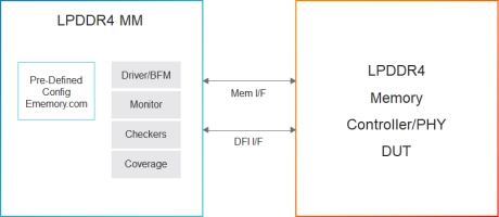
Simulation VIP for LPDDR4
- Speed (Mt/s)
- 2133MHz (4266MT/s)
- Device Density
- Supports a wide range of device densities from 4Gb to 32Gb