Flash Memory IP
Filter
Compare
277
IP
from
67
vendors
(1
-
10)
-
Flash Memory LDPC Decoder IP Core
- Quasi cyclic (QC) – Algebraic constructed – LDPC Code
- Regular Parity Check Matrix
- Codeword length: 16 K
- Code rate 0.953
- No or very low error floor
- Parallel/Layered decoding
-
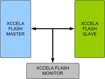
Xccela Flash Memory Model
- Supports Xccela Flash memory devices like MT35X_QLJW_U_256_ABA/ MT35X_QLKA_L_01G_BBA/ MT35X_QLKA_U_02G_CBA from all leading vendors
- Supports 100% of Xccela Flash protocol Standards.
- Supports all the Xccela Flash commands as per the specs.
- Supports Single and double transfer rate (SDR/DDR)
-
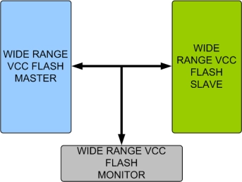
Wide Range VCC Flash Memory Model
- Supports Wide Range VCC Flash memory devices like MX25R3235F, MX25R1635F, MX25R6435 from all leading vendors
- Supports 100% of Wide Range VCC Flash protocol standards.
- Supports all the Wide Range VCC Flash commands as per the specs.
- Supports Serial Peripheral Interface - Mode 0 and Mode 3
-
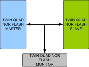
Twin Quad NOR Flash Memory Model
- Supports Twin Quad NOR Flash memory devices like MT25T_QLKT_L_01G_xBB from all leading vendors
- Supports 100% of Twin Quad NOR Flash protocol standards.
- Supports all the Twin Quad NOR Flash commands as per the specs.
- Supports Stacked device (two 512Mb die)
-
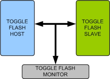
Toggle Flash Memory Model
- Compliant with Toggle Flash JESD230/ JESD230A/ JESD230B/ JESD230C/ JESD230D specifications.
- Supports SDR, Synchronous DDR, NV-DDR2 and Toggle-mode DDR data interface.
- Supports all mandatory and optional commands.
- Supports 16 bit bus width operations.
-
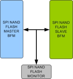
SPI NAND Flash Memory Model
- Fully compatible with SPI Nand Flash standards.
- Follows Nand Flash specification as defined in Micron specifications.
- Supports all commands as per specifications.
- Supports Master and Slave Mode
-
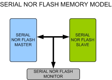
Serial NOR Flash Memory Model
- Supports Serial NOR Flash memory devices like MT25QL128ABA, MT25QL512ABA, MX25L12835F, MX25L25635F, N25Q032A from all leading vendors like Macronix, Micron, Winbond and many more.
- Supports 100% of Serial NOR Flash protocol.
- Supports all the Serial NOR Flash commands as per the specs.
- Supports Single and Double Transfer Rate (STR/DTR).
-
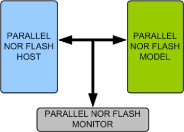
Parallel NOR Flash Memory Model
- Supports Parallel NOR Flash memory devices from all leading vendors.
- Supports 100% of Parallel NOR Flash protocol standard.
- Supports all the Parallel NOR Flash commands as per the specs.
- Supports Asynchronous random/page read
-
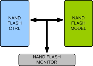
NAND Flash Memory Model
- Supports NAND Flash memory devices from all leading vendors.
- Supports 100% of NAND FLASH protocol standard of HY27UH08AG(5/D)M.
- Supports all the NAND FLASH commands as per the specs.
- Provides cost effective solutions for mass storage applications.
-
Flash Memory LDPC
- Irregular parity check matrix
- Layered decoding
- Minimum sum algorithm
- Soft decision decoding