DDR memory controller IP
Filter
Compare
334
IP
from
41
vendors
(1
-
10)
-
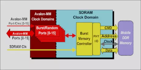
Avalon Mobile DDR Memory Controller
- 200 MHz Cyclone / Stratix memory performance
- Supports all standard Mobile DDR SDRAM devices
- 1 to 16 Avalon® independent local bus port interfaces
- Avalon Pipelined and Burst transfers
-
DO-254 DDR Memory Controller 1.00a
- DDR, DDR2, DDR3, and LPDDR (Mobile DDR) memory standards support
- Up to 800 Mb/s (400 MHz double data rate) performance
- Up to four MCB cores in a single Spartan-6 device
- Configurable dedicated multi-port user interface to FPGA logic
-
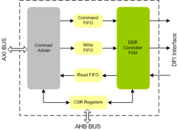
DDR Memory Controller IP for low power and high reliability
- Supports DDR protocol standard JESD79F Specification.
- Compliant with DFI-version 2.0 or higher Specification.
- Supports all the DDR commands as per the specs. Supports up to 16 AXI ports with data width upto 512 bits.
- Supports controllable outstanding transactions for AXI write and read channels
-
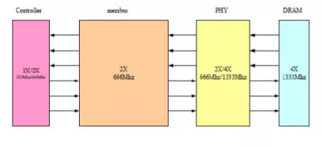
High Performance DDR 3/2 Memory Controller IP
- Supports DDR3/DDR2 SDRAM
- 16 bits width DDR2/DDR3 SDRAM Interface
- Memory Clock up to 462MHz, DFI Clock up to 462MHz
- Support DDR2 667/800/1066 and DDR3 667/800/1066/1333/1600/1866
-
DDR 4/3 Memory Controller IP - 2400MHz
- Support s DDR 4 /DDR3 SDRAM
- 16 bit s width , Single Channel DDR 4 /DDR3 SDRAM Interface .
- 16 bits for per channel, could support 2 x8 bits DDR3, but could not support 2 x8 bits DDR4.
- Memory Clock up to 6 66 MHz, DFI Clock up to 666 MHz .
-
SDRAM DDR Controller
- Dolphin Technology offers high performance DDR4/3/2 SDRAM and LPDDR5/4x/4/3/2 SDRAM Memory Controller IP across a broad range of process technologies.
-
PSRAM Memory Controller IP
- DFSPI – SPI FLASH Controller with Execute in place – XIP (SINGLE, DUAL and QUAD SPI Bus Controller with DDR / DTR support and optional AES Encryption) + … NOR & NAND Flash Memory Support
-
High-Performance Memory Controller II SDRAM Intel® FPGA IP Core
- The High-Performance Memory Controller II SDRAM Intel FPGA IP core handles the complex aspects of using DDR, DDR2, and DDR3 SDRAM at speeds up to 933 MHz
- The intellectual property (IP) core initializes the memory devices, manages SDRAM banks, translates read-and-write requests from the local interface into all the necessary SDRAM command signals, and performs command and data reordering.

-
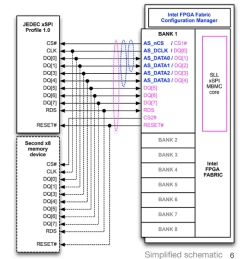
xSPI Multiple Bus Memory Controller
- SLL’s unified xSPI Multiple Bus Memory Controller IP supports the widest range of JEDEC xSPI and xSPI-like NOR Flash and PSRAM memories (JEDEC xSPI Profile 1.0 and 2.0, HyperBus 1.0, 2.0 and 3.0, OctaBus and Xccela Bus) that are available now from many memory vendors.
- JEDEC xSPI and xSPI-like memories offer good performance with lower hardware and power costs. Memory device variants offer up to 512 Mbit PSRAM, up to 2 Gigabit NOR Flash, up to 250 MHz DDR clock speeds, with x4, x8 and x16 data path widths, and a wide range of package options including 4mm x 4mm BGA49 and tiny WLCSP footprints. Some PRSAM devices are now also available with internal ECC.
-
DDR Controller IIP
- Supports DDR protocol standard JESD79F Specification.
- Compliant with DFI-version 2.0 or higher Specification.
- Supports all the DDR commands as per the specs.
- Supports up to 16 AXI ports with data width upto 512 bits.