LVDS IP for TSMC
Welcome to the ultimate
LVDS IP
for
TSMC
hub! Explore our vast directory of
LVDS IP
for
TSMC
All offers in
LVDS IP
for
TSMC
Filter
Compare
80
LVDS IP
for
TSMC
from
14
vendors
(1
-
10)
-
LVDS Deserializer IP
- The MXL-DS-LVDS is a high performance 4-channel LVDS Deserializer implemented using digital CMOS technology.
- Both the serial and parallel data are organized into four channels. The parallel data can be 7 or 10 bits wide per channel. The input clock is 25MHz to 165MHz. The De-serializer is highly integrated and requires no external components.
-
LVDS Serializer IP
- The MXL-SR-LVDS is a high performance 4-channel LVDS Serializer implemented using digital CMOS technology. Both the serial and parallel data are organized into four channels.
- The parallel data width is programmable, and the input clock is 25MHz to 165MHz. The Serializer is highly integrated and requires no external components.
-
MIPI D-PHY/LVDS Combo Receiver IP
- The MXL-LVDS-MIPI-RX is a high-frequency, low-power, low-cost, source-synchronous, Physical Layer that supports the MIPI® Alliance Standard for D-PHY and compatible with the TIA/EIA-644 LVDS standard.
- The IP is configured as a MIPI slave and consists of 5 lanes: 1 Clock lane and 4 data lanes, which make it suitable for display serial interface applications (DSI).
-
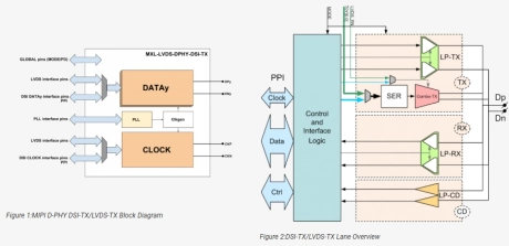
MIPI D-PHY/LVDS Combo Transmitter IP
- The MXL-LVDS-DPHY-DSI-TX is a combo PHY that consists of a high-frequency low-power, low-cost, source-synchronous, Physical Layer supporting the MIPI® Alliance Standard for D-PHY and a high performance 4-channel LVDS Serializer implemented using digital CMOS technology.
- In LVDS mode, both the serial and parallel data are organized into 4 channels. The parallel data is 7 bits wide per channel. The input clock is 25MHz to 150MHz. The serializer is highly integrated and requires no external components. The circuit is designed in a modular fashion and desensitized to process variations. This facilitates process migration, and results in a robust design.
-
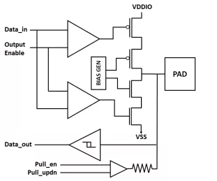
Ultra-low leakage I/O Library in TSMC 22nm
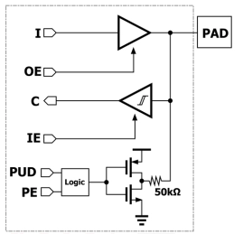
- A TSMC 22nm Wirebond I/O Library with ultra-low leakage 1.8V GPIO, 1.8V I2C ODIO, 1.8V analog cell and associated ESD.
- This is an ultra-low leakage library. The GPIO has a typical leakage of only 150pA from VDDIO and 1nA from VDD.
- The library has a GPIO and an ODIO. The GPIO cell set can be configured as input or output and has an internal 50K ohm pull-up or pull-down resistor.
-
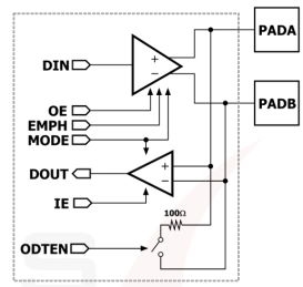
2Gbps LVDS/SVLS Combo Transceiver in TSMC 16nm
- AD_SLVS_LVDS is a highly configurable 2Gbps transceiver for LVDS or SLVS interfaces. With features like dynamic interface selection, on-die termination and pre-emphasis, this I/O is flexible enough for any system.
- To compliment this I/O, the vendor also offers a accompanying silicon-proven ESD and GPIO pad library in TSMC 12/16nm.
- This I/O provides 2kV HBM protection but can be extended up to 8kV upon request.
-
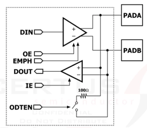
LVDS Transceiver in TSMC 28nm
- This 1.8V LVDS transceiver, designed for TSMCs 28nm process, delivers high-speed, low-power differential signaling with superior signal integrity.
- Engineered with 1.8V thick oxide devices and a 0.8V standard core interface, it operates ef- ficiently across a wide temperature range (-40°C to 125°C).
-
1.8V/3.3V Switchable GPIO with I2C, HDMI, LVDS, ESD & Analog in TSMC 28nm
- A TSMC 28nm HPM/HPC/HPC+ Wirebond I/O Library with a switchable 1.8V/3.3V GPIO, 5V I2C ODIO, 1.8V & 3.3V Analog Cells, ESD and more.
- A key attribute of this silicon-proven library is to detect and adjust to a VDDIO supply of 1.8V or 3.3V during system operation.
- The GPIO can be configured as input, output, open-source, or open-drain with an optional 60kohm pull-up or pull-down resistor.
-
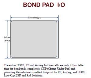
HDMI, LVDS, RF and Analog Pads in TSMC 45/40nm
- A 1.0V to 5V Analog I/O library that includes an HDMI, LVDS, and Analog/RF Low Capacitance pad set in TSMC 45/40nm HPM process.
- This library is collection of analog only IO and Power/Ground pads that include ESD. The target applications are high performance analog interfaces including HDMI, RF, LVDS, basic analog and other applications.
- The pads include a host of specialty features including fail safe, low capacitance, high ESD protection, and IEC robustness.
-
2.5V GPIO with 2Gbps LVDS RX TX and Analog Cell in GlobalFoundries 65nm LPe
- A GlobalFoundries 65nm LPE Wirebond I/O library with 2.5V GPIO, 2Gbps LVDS TX RX and 2.5V Analog/RF cell with associated ESD.
- A key attribute of this silicon-proven library include dual selectable drive strengths and independent input & output enable / disable.
- The GPIO cell can be configured as input, output or open-drain with a Schmitt trigger input and selectable internal 60K ohm pull-up or pull-down resistor.