I/O Library IP for TSMC
Welcome to the ultimate
I/O Library IP
for
TSMC
hub! Explore our vast directory of
I/O Library IP
for
TSMC
All offers in
I/O Library IP
for
TSMC
Filter
Compare
333
I/O Library IP
for
TSMC
from
19
vendors
(1
-
10)
-
HDMI, LVDS, RF and Analog Pads in TSMC 45/40nm
- A 1.0V to 5V Analog I/O library that includes an HDMI, LVDS, and Analog/RF Low Capacitance pad set in TSMC 45/40nm HPM process.
- This library is collection of analog only IO and Power/Ground pads that include ESD. The target applications are high performance analog interfaces including HDMI, RF, LVDS, basic analog and other applications.
- The pads include a host of specialty features including fail safe, low capacitance, high ESD protection, and IEC robustness.

-
TSMC 22ULL 1.8V/3.3V SD/eMMC PHY AG2
- Synopsys SD/eMMC PHY provides an optimal balance for cost and performance for storage solutions
- Synopsys SD/eMMC PHY is a hard IP that can be used to implement a single interface that can accomplish 4-bit, 8-bit eMMC & 4-bit SD operations
- It includes an optional digi logic circuitry which is required for high-speed operations
- It complies with eMMC 5.1 (JESD84-B51A) and SDIO 6.0 JEDEC standards

-
TSMC N3E SD/eMMC PHY North/South Poly Orientation
- Synopsys SD/eMMC PHY provides an optimal balance for cost and performance for storage solutions
- Synopsys SD/eMMC PHY is a hard IP that can be used to implement a single interface that can accomplish 4-bit, 8-bit eMMC & 4-bit SD operations
- It includes an optional digi logic circuitry which is required for high-speed operations
- It complies with eMMC 5.1 (JESD84-B51A) and SDIO 6.0 JEDEC standards

-
TSMC N3P SD/eMMC PHY North/South Poly Orientation
- Synopsys SD/eMMC PHY provides an optimal balance for cost and performance for storage solutions
- Synopsys SD/eMMC PHY is a hard IP that can be used to implement a single interface that can accomplish 4-bit, 8-bit eMMC & 4-bit SD operations
- It includes an optional digi logic circuitry which is required for high-speed operations
- It complies with eMMC 5.1 (JESD84-B51A) and SDIO 6.0 JEDEC standards

-
TSMC N5 SD/eMMC PHY North/South Poly Orientation
- Synopsys SD/eMMC PHY provides an optimal balance for cost and performance for storage solutions
- Synopsys SD/eMMC PHY is a hard IP that can be used to implement a single interface that can accomplish 4-bit, 8-bit eMMC & 4-bit SD operations
- It includes an optional digi logic circuitry which is required for high-speed operations
- It complies with eMMC 5.1 (JESD84-B51A) and SDIO 6.0 JEDEC standards

-
TSMC N4P SD/eMMC PHY North/South Poly Orientation
- Synopsys SD/eMMC PHY provides an optimal balance for cost and performance for storage solutions
- Synopsys SD/eMMC PHY is a hard IP that can be used to implement a single interface that can accomplish 4-bit, 8-bit eMMC & 4-bit SD operations
- It includes an optional digi logic circuitry which is required for high-speed operations
- It complies with eMMC 5.1 (JESD84-B51A) and SDIO 6.0 JEDEC standards
-
M31 eMMC/SDIO at TSMC 22ULL Process
- Supports HS400 (400Mbps), HS200 (200Mbps), High-speed DDR (52Mbps) and etc.
- Consisting of driver, receiver & pull-up/down resistors
- Power-sequence free
- Provides multi-driving-strength selection
-
M31 eMMC/SDIO at TSMC 22ULP Process
- Supports HS400 (400Mbps), HS200 (200Mbps), High-speed DDR (52Mbps) and etc.
- Consisting of driver, receiver & pull-up/down resistors
- Power-sequence free
- Provides multi-driving-strength selection

-

-
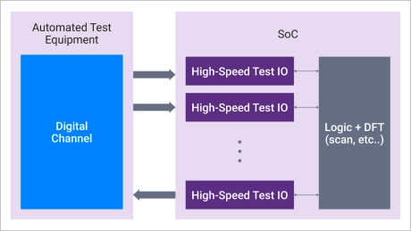
TSMC N3P 1.2V High-Speed Test IO
- The AI and HPC industries are advancing toward chiplet-based designs to achieve superior performance, as traditional monolithic SoCs face scaling challenges
- Heterogeneous integration is driving semiconductor innovation but adds complexity to chip design, requiring advanced testing methodologies and improved Automated Test Equipment (ATE)
- Increasing test patterns and limited package pins demand high-bandwidth IOs, while advancements in ATE capabilities further necessitate optimized GPIOs to support higher-speed, efficient and low-cost testing
- Synopsys High-Speed Test IO IP is a cutting-edge IO interface solution that enables efficient, high-speed testing of complex semiconductor designs while minimizing hardware complexity and cost