Interface IP Cores for GLOBALFOUNDRIES
-
32Gbps SerDes PHY in GF 22nm
- This 32Gbps SerDes PHY is implemented in GlobalFoundries 22FDX CMOS technology and provides a high-performance, protocol-agnostic serial interface for advanced mixed-signal and high-speed digital SoCs.
- The PHY is architected as a modular design consisting of a low-jitter clock multiplier, a half-rate transmitter with digitally programmable feed-forward equalization, and a configurable CTLE-based receiver with digital clock-and-data recovery, supporting both 16 Gbps and 32 Gbps operation.
-
USB Full Speed Transceiver
- Exceeds USB 2.0 Full Speed specification.
- Trimmed pull up resistor.
- Enable / suspend feature.
- DPF and UFP options available.
-
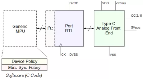
Complete USB Type-C Power Delivery IP
- Mixed signal Analog Front End Macros for 65n, 130n, 150nm, and 180n technologies.
- RTL code from AFE to I2C compatible register set.
- Stand alone C code for Protocol, Device Policy Manager, and System Policy Manager.
- IP demonstration & development board, with compliance reports.
- Full chip integration of USB Type-C, and associated software.
-
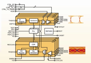
4.25 Gbps Multi-Standard SerDes
- The MXL4254A is a silicon proven Quad Gigabit SerDes implemented in digital CMOS technology. Each of the four channels supports data rate up to 4.25 Gbps.It is compatible with router-backplane links, PCI Express, SATA, RapidIO, 10 Gbps Ethernet (XAUI), FibreChannel, SFI-5, SPI-5, and other communication applications.
-
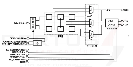
Ultra-short reach SerDes with 500 Gbit/s throughput
- 2x to 4x throughput at 50% or less energy consumption as compared to conventional SerDes over the same number of pins/wires
- High pin-efficiency and low power
- 208.3 Gbit/s full-duplex bandwidth per mm of die edge (500 Gbit/s for 2.4 mm of die edge)
-
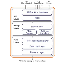
PCIe 3.1 Controller with AXI
- Compliant with the PCI Express 3.1/3.0, and PIPE (16- and 32-bit) specifications
- Compliant with PCI-SIG Single-Root I/O Virtualization (SR-IOV) Specification
- Supports Endpoint, Root-Port, Dual-mode configurations
- Supports x16, x8, x4, x2, x1 at 8 GT/s, 5 GT/s, 2.5 GT/s speeds
- Supports AER, ECRC, ECC, MSI, MSI-X, Multi-function, P2P, crosslink, and other optional features
- Supports many ECNs including LTR, L1 PM substates, etc.
-
I2C Controller IP – Master, Parameterized FIFO, AXI Bus
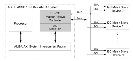
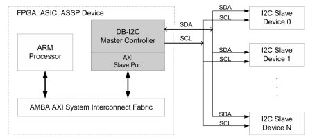
- The DB-I2C-M-AXI Controller IP Core interfaces an ARM, MIPS, PowerPC, ARC or other high performance microprocessor via the AMBA 2.0 AXI System Interconnect Fabric to an I2C Bus. The I2C is a two-wire bidirectional interface standard (SCL is Clock, SDA is Data) for transfer of bytes of information between two or more compliant I2C devices, typically with a microprocessor behind the master controller and one or more slave devices.
- The DB-I2C-M-AXI is a Master I2C Controller that controls the Transmit or Receive of data to or from slave I2C devices. Figure 1 depicts the system view of the DB-I2C-M AXI Controller IP Core embedded within an integrated circuit device.
-
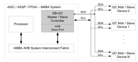
I2C Controller IP- Master / Slave, Parameterized FIFO, AHB Bus
-
The DB-I2C-MS-AHB Controller IP Core interfaces a microprocessor via the AMBA AHB Bus to an I2C Bus in Standard-Mode (100 Kbit/s) / Fast-Mode (400 Kbit/s) / Fast-Mode Plus (1 Mbit/s) / Hs-Mode (3.4+ Mb/s) / Ultra Fast-Mode (5 mbit/s).
The I2C is a two-wire bidirectional interface standard (SCL is Clock, SDA is Data) for transfer of bytes of information between two or more compliant I2C devices, typically with a microprocessor behind the master controller and one or more slave devices.
The DB-I2C-MS-AHB is a Master / Slave I2C Controller that in Master Mode controls the Transmit or Receive of data to or from slave I2C devices while in Slave Mode allows an external I2C Master device to control the Transmit or Receive of data.
-
-
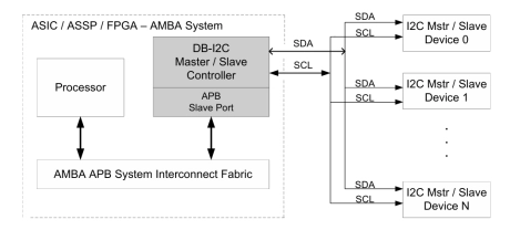
I2C Controller IP- Master / Slave, Parameterized FIFO, APB Bus
-
The Digital Blocks DB-I2C-MS-APB Controller IP Core interfaces a microprocessor via the AMBA APB Bus to an I2C Bus in Standard-Mode (100 Kbit/s) / Fast-Mode (400 Kbit/s) / Fast-Mode Plus (1 Mbit/s) / Hs-Mode (3.4+ Mb/s) / Ultra Fast-Mode (5 mbit/s).
The I2C is a two-wire bidirectional interface standard (SCL is Clock, SDA is Data) for transfer of bytes of information between two or more compliant I2C devices, typically with a microprocessor behind the master controller and one or more slave devices.
The DB-I2C-MS-APB is a Master/Slave I2C Controller that in Master Mode controls the Transmit or Receive of data to or from slave I2C devices while in Slave Mode allows an external I2C Master device to control the Transmit or Receive of data.
-
-
I2C Controller IP- Master / Slave, Parameterized FIFO, AXI Bus
- The DB-I2C-MS-AXI Controller IP Core interfaces a microprocessor via the AMBA AXI Bus to an I2C Bus in Standard-Mode (100 Kbit/s) / Fast-Mode (400 Kbit/s) / Fast-Mode Plus (1 Mbit/s) / Hs-Mode (3.4+ Mb/s) / Ultra Fast-Mode (5 mbit/s).
- The I2C is a two-wire bidirectional interface standard (SCL is Clock, SDA is Data) for transfer of bytes of information between two or more compliant I2C devices, typically with a microprocessor behind the master controller and one or more slave devices.
- The DB-I2C-MS-AXI is a Master / Slave I2C Controller that in Master Mode controls the Transmit or Receive of data to or from slave I2C devices while in Slave Mode allows an external I2C Master device to control the Transmit or Receive of data.