Protecting die-2-die interfaces...

There are several reasons to combine various chiplets in a single package, either next to each other (2.5D) or stacked on top of each other (3D) like the memory cube depicted below.
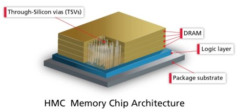
Example of a 3D stacked, co-packaged assembly. 4 layers of DRAM memory are stacked on top of a logic layer. Many of the interfaces between the logic layer and the memory devices stay within the package.
For instance, it enables chip designers to select the most optimal process for each type of function (interface, memory, compute, FPGA, analog circuits, MEMS, optical, …). It also allows to create chips with larger gate count when the reticle size is the limiting factor. And of course, yield improves a lot when the area of the die is reduced.
At Sofics we get a lot of questions about the required ESD robustness for the die-2-die (D2D) interfaces between chiplets in a package. People wonder how to select the right ESD standard (HBM, MM, CDM, TLP – more info) and what robustness level (1kV HBM?) they need to design for. Furthermore people wonder how they can validate the robustness once ESD devices are integrated?
What is the right ESD standard and ESD robustness level?
To read the full article, click here
Related Semiconductor IP
- HBM4 PHY IP
- Ultra-Low-Power LPDDR3/LPDDR2/DDR3L Combo Subsystem
- HBM4 Controller IP
- IPSEC AES-256-GCM (Standalone IPsec)
- Parameterizable compact BCH codec
Related Blogs
- SSD Interfaces and Performance Effects
- Protecting Against IP Theft
- On-chip interfaces gain importance in next-gen FPGAs
- Verifying MIPI interfaces in SoCs
Latest Blogs
- Formally verifying AVX2 rejection sampling for ML-KEM
- Integrating PQC into StrongSwan: ML-KEM integration for IPsec/IKEv2
- Breaking the Bandwidth Barrier: Enabling Celestial AI’s Photonic Fabric™ with Custom ESD IP on TSMC’s 5nm Platform
- What Does a GPU Have to Do With Automotive Security?
- Physical AI at the Edge: A New Chapter in Device Intelligence