Same Chip, Two Destinies: How Power Profiles Improve With On-Chip Monitoring

The impact of in-chip telemetry on peak power, average power, and Di/Dt noise
What happens to critical power-related considerations when the same chip is handled two different ways, with or without visibility from within?
This article begins by examining how the absence of on-chip monitoring impacts peak power, average power, and Di/Dt noise (rate of current change), as illustrated in the diagram below and the subsequent discussion. It then details how these aspects change when in-chip telemetry is available.
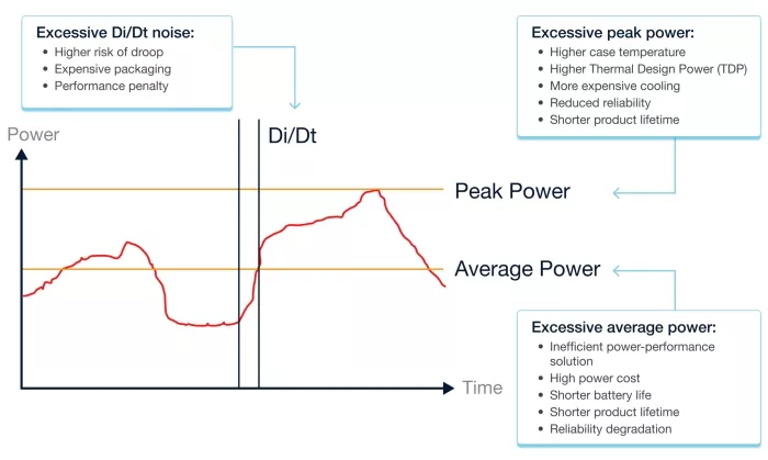
Fig. 1: As the power profile shifts with different modes and switching activity, high Di/Dt noise, peak power, and average power introduce thermal, cost, and reliability penalties.
On-Chip Telemetry OFF: Excessive Peak Power
To improve power and performance specs while reducing chip operational costs, engineers must determine the lowest reliable voltage, known as VDDmin, at a certain frequency of operation, which varies significantly between dies due to the process distribution.
Without on-chip telemetry, chipmakers typically detect VDDmin using VDD search testing, which lowers the voltage step by step until chip failure occurs to identify the last functional VDD. However, this method presents a difficult tradeoff:
- Smaller voltage steps improve accuracy but increase test time.
- Larger voltage steps are quicker but might overshoot the optimal point.
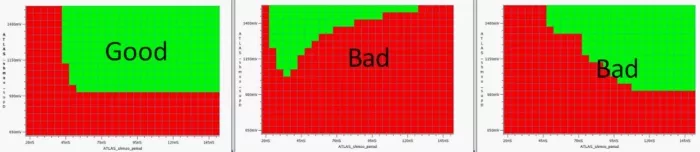
Fig. 2: Voltage search plots. Determining an accurate VDDmin using this method often requires an impractically long time and high test cost, leading to painful compromises.
As a compromise, many chipmakers divide all chips into a few bins, such as slow/fast/typical, setting a single voltage level per bin. However, due to the substantial variation in each bin, many units are assigned higher-than-required VDDmin, leading to excessive peak power and power density that have significant downsides, including:
- Higher case temperature (Tcase)
- Higher Thermal Design Power (TDP)
- More expensive cooling
- Reduced reliability
- Shorter product lifetime
TDP dictates the form factor, cooling architecture, and rack density. When chips operate above their true minimum voltage, dynamic power increases sharply. That power converts to heat, resulting in higher TDP, expensive cooling solutions, higher failure rates, and shorter lifetime.
On-Chip Telemetry OFF: Excessive Di/Dt noise
Current spikes go undetected without on-chip telemetry, forcing engineers to compensate with increasing chip cost due to more expensive packaging, on-die/off-die decoupling capacitance, and on-die active droop mitigation solutions that are designed to absorb Di/Dt noise and reduce voltage droop. But that cost is only part of the tradeoff. Without visibility into current transients, designers must raise voltage or apply large safety margins to prevent failures in marginal paths.
These decisions suppress frequency and harm performance. Meanwhile, higher power turns into heat, increasing cooling demands and pushing thermal limits.
What begins as an invisible current fluctuation ends in performance loss and higher costs:
- Higher risk of droop
- Cost
- Performance penalty
On-Chip Telemetry OFF: Excessive Average Power
Without on-chip monitoring, voltage adjustment in the field relies on guesswork rather than real timing data. Typically, Adaptive Voltage Scaling (AVS) uses canary circuits based on ring oscillators (ROSC). This method attempts to mimic critical paths but fails to reflect actual workload and reliability stress, or aging effects on the real logic.
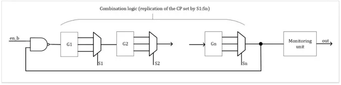
Fig. 3: A canary circuit that monitors design margins is a critical path replicator, which cannot provide accurate data about actual critical path timing.
To compensate for the inaccuracy, designers must apply conservative guard bands to prevent failures, leading to higher voltages that cause excessive average power and reduced performance.
These overprotective settings inflate operational costs and compromise long-term reliability, while offering no visibility into when and where timing issues may arise.
Excessive average power also affects performance by raising thermal load and limiting voltage-frequency optimization. Both effects force the system to reduce operating frequency to remain within power and thermal limits.
The effects of excessive average power carry several long-term drawbacks:
- Inefficient power-performance solution
- High power cost
- Shorter battery life (when applicable)
- Shorter product lifetime
- Reliability degradation
Power optimization: A solution that sees what others can’t
Chipmakers face three power-related constraints in every design: peak power, average power, and Di/Dt. Without visibility into real device behavior, these factors are managed through best known assumptions and worst-case settings.
To compensate for these blind spots, engineers divide dies into broad voltage bins, apply conservative voltage guard bands, and use expensive packages designed to absorb transient noise.
These choices increase test time, inflate cost, reduce performance, and shorten system life, among other drawbacks.
To address these severe implications, proteanTecs has introduced a novel approach with its on-chip Agents, which are specialized monitoring IPs embedded during design. These Agents provide accurate measurements of critical parameters such as real logic timing margins during actual operation.
The rich telemetry data can also feed the proteanTecs advanced data analytics software, including ML models, to guide vital decisions throughout the device production lifecycle. This level of accuracy enables meaningful reductions in cost, greater reliability, and measurable improvements in power and performance.
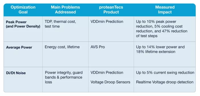
Table 1: The impact of the proteanTecs on-chip monitoring solutions on three key optimization goals.
On-Chip Telemetry ON: Optimized Peak Power
With proteanTecs VDDmin Prediction for static operational voltage setting per device, voltage is accurately predicted per die and mapped to a much finer bin based on actual measured behavior. No more time-consuming voltage sweeps that lead to unnecessary overhead. Production cases have demonstrated ~ 70% reduction in test steps with no accuracy impact, resulting in decreased costs and accelerated time-to-market. This VDDmin prediction can be done both at the tester level and at the system level, using real application workloads.
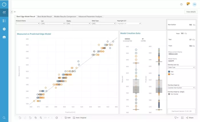
Fig. 4: proteanTecs VDDmin Prediction: Measured VDDmin (Y-axis) vs. predicted VDDmin (X-axis) comparison demonstrates exceptional accuracy with 0.15 NRMSE.
VDDmin Prediction is based on an ML model, trained on accurate data from the on-chip Agents. During chip-level high volume production testing, the model is integrated into the test program software and used in real time, per device, on the test floor – to predict the optimal voltage. The prediction is tested and after a minimal number of search steps, the operational voltage is fused in the device.
Voltage reduction has a substantial effect on peak power, which in turn lowers the Tcase and the cooling solution cost:
As peak power reduction translates to lower thermal load, it has a system-wide impact:
- Lower Tcase
- Lower TDP
- Cheaper cooling solution
- Better reliability
- Increased lifetime
For example, these are the quantified benefits when VDDmin Prediction reduces voltage by 3%-5%:
- ∆P [W] is within -6% to -10%
- ∆Tcase [°C] is within -3% to -5%
- ∆TDP [W] is within 3% to 5%
- ∆Cooling Cost [$] is within -3% to -5%
These optimizations are critical because cooling systems already consume 30% to 55% of datacenter power budgets. Reducing chip power directly cuts thermal load, which translates into real savings in infrastructure.
In high-density racks, advanced liquid cooling can cost between $1,000 and $2,000 per kW cooled, which can add up to millions of dollars annually. Every watt saved at the silicon level reduces that burden.
On-Chip Telemetry ON: Optimized Di/Dt Noise
High current swings trigger voltage droop, which can disrupt timing and cause failures. In the absence of accurate real-time monitoring, engineers compensate by using higher voltages, wider margins, on-die droop mitigation solutions (that incur performance penalty), and die cost to absorb these transients.
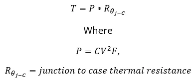
proteanTecs VDDmin Prediction makes these compensations unnecessary\y by lowering VDD per die, which improves signal integrity through reduced current swings and Di/Dt noise. Lower voltage also makes room for higher frequencies that boost performance, as captured by this equation:

These improvements enable:
- Safer operation (reduced noise)
- Cheaper package
- Better performance
For example, these are the quantified benefits when VDDmin Prediction reduces voltage by 3%-5%:
- ∆I [mA] is within -3% to -5%
- ∆Vnoise [mV] is within -3% to -5%
- ∆F [MHz] is within 3% to 5%
In addition, proteanTecs provides real-time voltage droop sensors to protect the device in mission-mode. They provide real-time hardware signals that can trigger a clock throttling event to avoid failure and reduce Di/Dt.
On-Chip Telemetry ON: Optimized Average Power
Unlike canary circuits, proteanTecs AVS Pro uses Agents that monitor true logic paths for more informed decisions. proteanTecs’ technology allows high coverage of the performance limiters, allowing precise guard-band tuning based on real workloads, aging, and IR drops.
This approach enables safer voltage scaling, avoiding worst-case guard-bands and allowing the device to operate closer to its actual limits without compromising functionality, performance and reliability. As demonstrated below, AVS Pro safely reduced power consumption of a production 5nm SoC by 12.5%. At the same time, it extended the predicted lifetime by 18%.
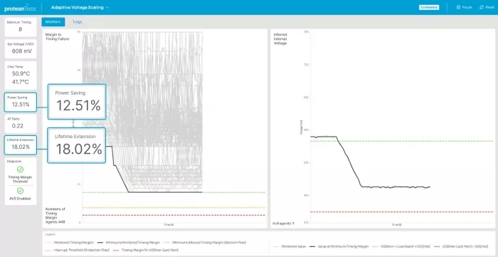
Fig. 5: AVS Pro, visualized here, enables 12.51% power saving through safer voltage scaling, leading to 18% projected lifetime extension.
proteanTecs AVS Pro continuously adjusts voltage based on real-time Agent data. As the device operates with a surplus of timing margin, AVS Pro reduces the voltage. When more stressful functional workloads operate or degradation reduces timing margins, AVS Pro increases the voltage only as much as needed to maintain safe operation.
This continuous response avoids both oversupply and undershoot, providing substantial benefits:
- Optimized power-performance
- Reduced power cost
- Higher battery life (when applicable)
- Increased lifetime
- Better reliability
The chart below shows how AVS Pro delays degradation over time. The device maintains safe performance levels for longer, pushing the wear-out point further into the product lifecycle.
This type of lifetime extension has significant financial implications. Hyperscalers like Amazon, Alphabet, and Microsoft publicly attribute billions in annual net income to extending server lifespans by just one to two years. proteanTecs AVS Pro supports similar CAPEX reduction strategies by delaying degradation without compromising performance.
To learn more about the benefits of using AVS Pro for chip lifetime extension, read the full paper here.
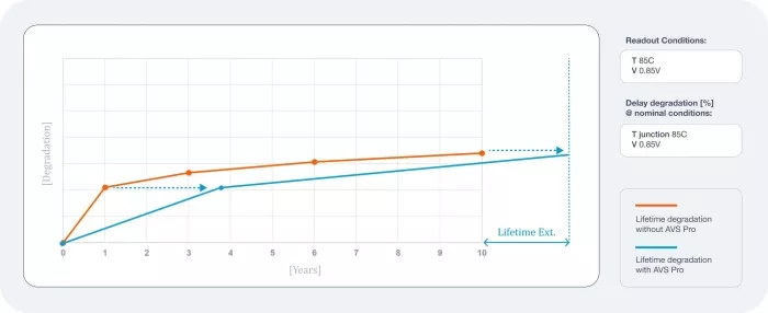
Fig. 6: An example of chip lifetime extension enabled by AVS Pro: 5nm delay degradation simulations [%] at nominal conditions: T junction 85 °C, V=0.75V
Conclusion – A tale of two chips
Many love underdogs, but as this article shows, products with on-chip telemetry win by a knockout.
proteanTecs provides visibility from within that spans production and deployment. With VDDmin Prediction and AVS Pro, power optimization begins at production test and continues throughout system operation.
VDDmin Prediction reduces peak power and Di/DT noise by tuning VDD with personalization and precision. Dedicated voltage droop sensors protect the device in real time, when unexpected workloads arrive. AVS Pro cuts average power through safer voltage scaling in the field. Together, they improve critical aspects of power, performance, and cost:
- For end users such as data center operators: lower energy costs, better performance, improved reliability, and longer lifetime.
- For system providers: lower system power, lower TDP, cheaper system that is also more compact, improved reliability, and longer lifetime.
- For chip vendors: improved power-performance, VDD Noise reduction, cheaper package, improved reliability, and longer lifetime.
Ready to realize the full benefits of on-chip telemetry? Contact our team here or download our whitepaper to see how proteanTecs enhances performance, efficiency, reliability, and product lifetime from test to deployment.
Related Semiconductor IP
- Power-OK Monitor
- SLM Signal Integrity Monitor
- SLM Clock & Delay Monitor IP
- Ultra‐Low‐Power Process/Voltage/Temperature Monitor on TSMC 16nm
- Ultra‐Low‐Power Process/Voltage/Temperature Monitor on TSMC 7nm FFC
Related Blogs
- Are low power and FPGA an oxymoron?
- ARM vs Intel...Performance? Power? OS support? Or ubiquity?
- PCI Express takes on Apple/Intel Thunderbolt and 16 Gtransfers/sec at PCI SIG while PCIe Gen 3 starts to power up
- Power To The IP Players
Latest Blogs
- Physical AI at the Edge: A New Chapter in Device Intelligence
- Rivian’s autonomy breakthrough built with Arm: the compute foundation for the rise of physical AI
- AV1 Image File Format Specification Gets an Upgrade with AVIF v1.2.0
- Industry’s First End-to-End eUSB2V2 Demo for Edge AI and AI PCs at CES
- Integrating Post-Quantum Cryptography (PQC) on Arty-Z7