GPIO Solutions for CERN’s Radiation-Hardened Applications

For over a decade, Sofics has collaborated with CERN, the European Organization for Nuclear Research. Sofics has delivered advanced GPIO cells tailored for radiation-hardened applications, supporting CERN’s groundbreaking particle physics experiments.
CERN’s Research and Electronics Requirements
CERN is at the forefront of particle physics research, striving to unravel the mysteries of the universe. Through their work, CERN has contributed immensely to our understanding of fundamental particles, forces, and interactions. Key experiments, such as those conducted at the Large Hadron Collider (LHC), involve high-energy collisions that yield new particles, pushing the boundaries of human knowledge.
CERN is a collaborative effort involving over 30 countries, emphasizing technological advancement, education, and the sharing of findings among nations. The focus is on understanding the very fabric of the universe, breaking matter down to its most elementary components—particles, fields, and interactions.
The journey into the smallest building blocks begins with molecules, which are made of atoms. Atoms consist of electrons orbiting a nucleus, which itself contains protons and neutrons. Delving even deeper, protons and neutrons are composed of quarks. CERN’s experiments aim to explore these elementary particles and the forces that govern them.
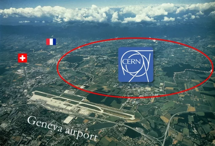
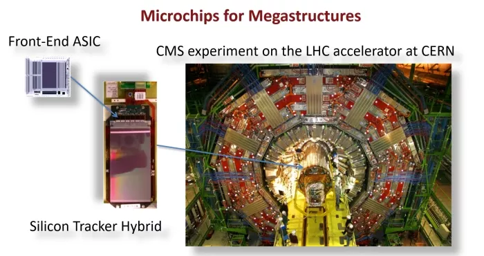
To study these particles, CERN has constructed the world’s “fastest racetrack”, the Large Hadron Collider (LHC). This 27-kilometer ring accelerates trillions of protons in two beams traveling in opposite directions at speeds approaching the speed of light. At specific points, the beams are directed to collide, creating conditions akin to those of the early universe.
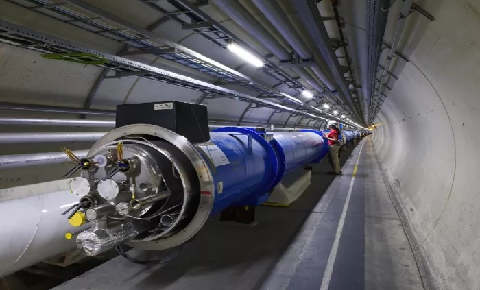
These collisions produce new particles, which are detected and analyzed using highly sophisticated electronic systems. The data gathered helps scientists piece together the nature of the universe, from its origins to its fundamental structure. For instance, such experiments led to the discovery of the Higgs boson, a breakthrough that revolutionized our understanding of particle physics..
These experiments demand highly reliable and precise electronics that can operate in extreme conditions, including radiation-heavy environments. The radiation in some experiments is up to 1000x the lethal dose for a human. the From detecting particle collisions to managing immense data streams, CERN’s electronic systems face unique challenges that require robust design and innovation.
Sofics’ Contributions to CERN’s Projects
Sofics and CERN have collaborated on multiple projects across various TSMC process nodes, including 130nm, 65nm, and 28nm CMOS technologies. For over a decade, Sofics has supplied CERN with radiation-hardened I/O libraries and ESD protection solutions to meet their stringent operational requirements.
CERN’s electronics need to withstand significant radiation exposure while maintaining functionality and reliability. Sofics has consistently delivered innovative I/O libraries and ESD protection solutions that are latch-up immune, exhibit low leakage, and meet area and capacitance constraints. These solutions play a vital role in CERN’s ability to gather and analyze critical data.
Case Study: 28nm RF HPC+ Technology Project
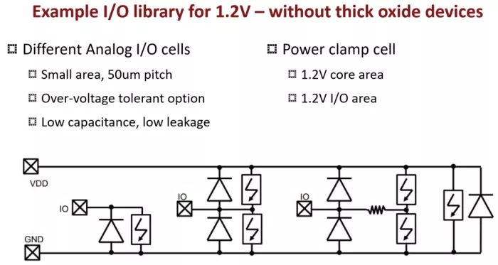
In one of the most recent collaborations, Sofics developed a 1.2V general-purpose I/O solution for CERN’s ASIC designs on TSMC 28nm RF HPC+ technology node. The challenge was to design radiation-tolerant 1.2V GPIOs using only 0.9V thin-gate MOS devices. It is important to avoid using thick-gate (1.8V) transistors that degrade in radiation-heavy environments. The radiation particles will be trapped in the thick oxide while flying through the thin 0.9V oxide. The thick oxide has a higher defect density where charges can remain trapped after radiation events. Trapped charges lead to increased leakage or even turn on the transistor permanently.
CERN’s specific requirements included a 1.2V signal for compatibility with existing ASICs, yet the standard TSMC 28nm GPIO library lacked a 1.2V option. Instead, it offered 0.9V core transistors and I/O transistors rated for 1.8V or 2.5V. This necessitated an innovative design approach to stack 0.9V transistors in both NMOS and PMOS configurations. Of course the circuit operation must ensure that the 0.9V limit across any two terminals is never exceeded. This involves generating bias voltages for the intermediate nodes.
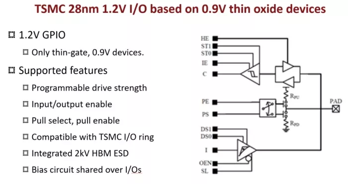
The 1.2V GPIO was designed fully compatible with the other I/O cells already in use by CERN, allowing seamless integration with CERN’s designs. The GPIO was also equipped with integrated 2kV HBM ESD protection to ensure reliability in extreme environments. Of course, also the ESD protection is not using any thick-oxide transistors. This solution not only ensured radiation tolerance but also integrated seamlessly with CERN’s existing systems, enabling reliable (1.2V) communication between their ASICs on more mature process nodes. The GPIO design came with typical features such as core isolation, programmable slew rate compensation, programmable drive strength, and input/output enable.
Design Architecture and Features
The architecture of this GPIO comprised several components:
- Digital Buffers and Level Shifters to interact with the core signals at core voltage levels.
- Receiver to translate high voltage analog bus signal to digital core signal
- ESD protection cells to mitigate damage from electrostatic discharge and electrical overstress.
- Driver to drive the bus signal, or high-Z mode.
- Bias Generator Blocks: These smaller circuits, capable of being shared across multiple I/Os, generated intermediate voltage levels for correct operation.
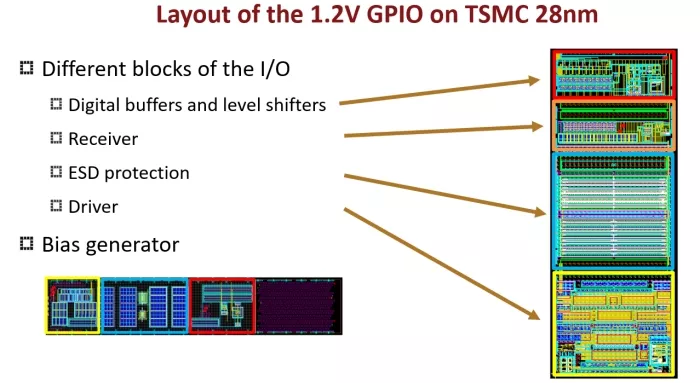
Each of these components has a modified architecture to allow voltages beyond the limit for the thin oxide transistors. While the design is created using thin oxide transistors the circuit has to ensure that these transistors remain in their Safe Operating Area (SOA). The datasheet can be downloaded here.
Scalability and Application
Sofics’ innovative design is not only limited to the 28nm node; the same architecture has been successfully applied to other process nodes. In the most advanced CMOS or FinFET processes the maximum I/O voltage is strongly reduced. In 7nm the highest voltage available in the GPIO library is only 1.8V. It is further reduced to 1.5 or 1.2V in 5nm/4nm FinFET technology.
Examples where Sofics engineers used the same circuit topology:
- 5V interface in 40nm technology, based on 3.3V transistors.
- 3.3V interface in 28nm CMOS based on stack of 1.8V I/O transistors
- 2.5V interface in 7nm FinFET technology using stacked 1.8V I/O transistors.
- 1.8V interface in 4nm using stacked 1.2V transistors
- 1.8V interface in 2nm technology using stacked 0.9V core transistors.
This achievement underscores Sofics’ expertise in creating innovative solutions for extreme environments, paving the way for continued advancements in high-performance semiconductor applications.
More background on the I/O circuits is available in a set of articles (I/O specs explained, Types of overvoltage tolerant I/O, Typical SOA violations in a stacked driver, overvoltage tolerant receiver structures).
Impact and Future Prospects
The collaboration between Sofics and CERN has empowered particle physics research by providing durable, high-performance electronics for demanding experiments. Sofics’ contributions have enabled CERN to collect and process critical data efficiently, furthering discoveries that benefit science and technology. Looking ahead, Sofics remains committed to supporting CERN’s ambitious research endeavors with continued innovation in radiation-hardened electronics.
Conclusion
The decade-long partnership between Sofics and CERN exemplifies the power of collaboration in overcoming extreme technical challenges. As CERN continues to push the boundaries of science, Sofics is proud to stand as a trusted partner, ready to deliver innovative solutions for future challenges.
Related Semiconductor IP
- Robust circuit and interface solutions
- On-chip ESD/EOS/Latch up/EMC protection for high voltage and BCD processes
- On-chip ESD/EOS/Latch up protection for advanced and low voltage processes
- TSMC N4P 1.2V/1.5V/1.8V GPIO Library MS add-on
- TSMC N4P 1.2V/1.5V/1.8V GPIO Library with 1.8V Failsafe MS Add-on
Related Blogs
- ARM furthers its "cover the earth" strategy with introduction of R5 and R7 core variants for fast, real-time, deterministic SoC applications
- Jeff Bier's Impulse Response - Mobile Application Processors Shift to Embedded Applications
- Synopsys Fields Processor Core for Neural Network Computer Vision Applications
- Speed, Function, and Technology as Key Factors for USB Applications
Latest Blogs
- Ensuring reliability in Advanced IC design
- A Closer Look at proteanTecs Health and Performance Management Solutions Portfolio
- Enabling Memory Choice for Modern AI Systems: Tenstorrent and Rambus Deliver Flexible, Power-Efficient Solutions
- Verification Sanity in Chiplets & Edge AI: Avoid the “Second Design” Trap
- Embedded Security explained: Cryptographic Hash Functions