Fabs foundries and fame

While our USP is in circuit and IP reuse, our ongoing engagement in technology transitions is almost as important. We’re working with all of the major names in the semiconductor industry to enable a cost-effective and high-quality transfer process.
There are a number of transition scenarios. For fabless companies and design houses, Thalia assists the development teams, helping them in the reuse of analog and mixed signal circuits and IPs with the AMALIA platform. The source and target foundry can be selected by the customer and qualified using Thalia’s Technology Analyzer, but Thalia also has the ability and expertise to advise on both node and foundry selection. Next, our experienced design team and proprietary Design Enabler is used to center the target design in the fastest and most efficient way.
On the other hand, for companies who prefer to use their own fabs and internal design teams, we offer our circuit and IP reuse platform adapted to their specific EDA environment (Cadence, Silvaco, Siemens EDA, Synopsys).
Quite often, IC design groups don’t have the in-house capabilities of a specialist company like Thalia to effectively adapt their EDA tools and tune their framework to specialised needs.
Figure 1: Examples of fab companies Thalia has worked with
In recent years our circuit and IP reuse platform has grown in popularity, largely because of the demonstrable benefits it delivers. These include:
- an efficient upfront qualification of the target process technology
- reduced design and redesign cycle time
- the swift generation of a portfolio of IPs.
We can also deliver improved performance, power and area of reused circuits and IPs.
Importantly too, we adapt the design reuse process to our customers’ needs. Thalia can take the full ownership of all aspects of migration or reuse including schematic architecture and layout and any re-centring or revisions that are needed.
Our business is to transition designs and our experienced designers, advanced methodologies and our automated AI based platform mean we are much more efficient and effective in this than many design houses. If we save up to 50 percent of the time that might otherwise be taken up in such a redesign, money is not only saved on worktime, redesign and people, but also on tools. The potential savings for our customers is in the order of tens of thousands of dollars - and we’re enjoying a lot of success.
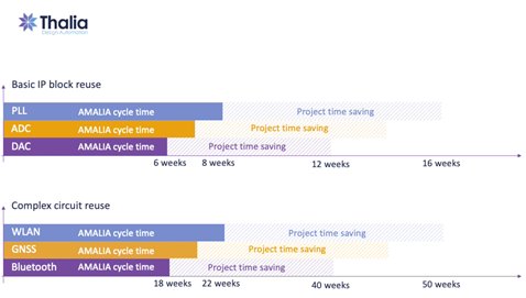
Figure 2: Examples of time savings delivered using AMALIA platform
Completing engagements faster and at less cost brings two significant additional benefits to our clients:
- Completing migrations faster means they are the first to market, gaining a competitive edge that is hard to overcome, and
- With lower development costs, return on investment is achieved much sooner. If costs are halved (for example) then the number of licenses of a given product that need to be sold to recoup development costs are vastly reduced.
A growing fame in a growing market and working with the worldwide foundry leader for many years, delivering fantastic results time and time again, we’re justifiably proud of what we are achieving.
Isn’t it time you found out what we could do for you?
Related Semiconductor IP
- LPDDR6/5X/5 PHY V2 - Intel 18A-P
- MIPI SoundWire I3S Peripheral IP
- P1619 / 802.1ae (MACSec) GCM/XTS/CBC-AES Core
- LPDDR6/5X/5 Controller IP
- Post-Quantum ML-KEM IP Core
Related Blogs
- TSMC Versus Global Foundries
- TSMC versus Global Foundries Part II
- Real men have fabs... or do they?
- Source of IP: Silicon foundries provides 18% of Design IP blocks, IP vendors only 16% to Fabless
Latest Blogs
- ML-DSA explained: Quantum-Safe digital Signatures for secure embedded Systems
- Efficiency Defines The Future Of Data Movement
- Why Standard-Cell Architecture Matters for Adaptable ASIC Designs
- ML-KEM explained: Quantum-safe Key Exchange for secure embedded Hardware
- Rivos Collaborates to Complete Secure Provisioning of Integrated OpenTitan Root of Trust During SoC Production