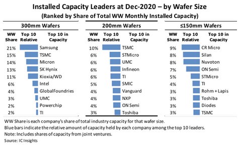
台积电在三个晶圆尺寸类别中产能均排名前十
New Global Wafer Capacity report shows top-10 installed capacity leaders in three different wafer size categories.
February 25, 2021 -- IC Insights recently released its new Global Wafer Capacity 2021-2025 report that provides details, analyses, and forecasts for IC industry capacity by wafer size, process geometry, region, and product type through 2025.
Rankings of IC manufacturers by installed capacity for each of the wafer sizes are shown in Figure 1. The chart also compares the relative amounts of capacity held by the top 10 leaders.

Figure 1
As of December 2020, only TSMC—the world’s largest foundry—was listed among the wafer capacity leaders in each of the three wafer size categories. It had the most 200mm wafer capacity last year and ranked second, trailing only Samsung, in 300mm wafer capacity.
It is not surprising that the 300mm ranking includes only DRAM and NAND flash memory suppliers like Samsung, Micron, SK Hynix, and Kioxia/WD; four of the world’s largest pure-play foundries TSMC, GlobalFoundries, UMC, and Powerchip (including Nexchip); and Intel, the industry’s biggest manufacturer of microprocessors. These companies offer the types of ICs that benefit most from using the largest wafer size available to best amortize the manufacturing cost per die. Moreover, they have the means to continue investing large sums of money in new and improved 300mm fab capacity.
Wafer capacity leaders in the 200mm size category consist of pure-play foundries and manufacturers that emphasize analog/mixed-signal ICs and microcontrollers.
The ranking for the smaller wafer sizes (i.e., ≤150mm) includes a more diversified group of companies, with two Chinese companies at the top. China Resources Microelectronics (CR Micro) and Silan Microelectronics both have very large 150mm fabs used mainly for the production of analog/mixed-signal ICs, power devices, and discrete semiconductors.
STMicroelectronics used to have a huge amount of 150mm wafer capacity for production of ICs at its fab site in Singapore but the company restructured its fab operations there in recent years. One fab was largely converted to manufacture MEMS-based microfluidic products (e.g., inkjet heads, lab-on-chip devices, etc.) and other fabs were upgraded to process 200mm wafers.
As the industry has moved IC fabrication onto larger wafers in bigger fabs, the number of IC manufacturers has continued to shrink. The Global Wafer Capacity study shows that as of December 2020, there were 63 companies that owned and operated a 200mm wafer fab (Figure 2). There were 28 companies that owned and operated a 300mm wafer fab. Furthermore, the distribution of 300mm wafer capacity among those manufacturers is top-heavy with the five biggest manufacturers controlling about three-quarters (74%) of the global 300mm IC capacity.

Figure 2
Report Details: Global Wafer Capacity 2021-2025
IC Insights’ Global Wafer Capacity 2021-2025—Detailed Analysis and Forecast of the IC Industry’s Wafer Fab Capacity report assesses the IC industry’s capacity by wafer size, minimum process geometry, technology type, geographic region, and device type through 2025. The report includes detailed profiles of the companies with the greatest fab capacity and gives comprehensive specifications on existing wafer fab facilities. Global Wafer Capacity 2021-2025 is priced at $4,890 for an individual user license. A multi-user worldwide corporate license is available for $7,590. The Internet access password and the information accessible to download will be available through November 2021.