IC制造商最大化300mm,200mm晶圆产能
A total of 25 new 300mm wafer fabs is expected between 2016 and 2021 as the outlook for 450mm wafers fades.
October 13, 2017 -- With the prospects of large 450mm wafers going nowhere, IC manufacturers are increasing efforts to maximize fabrication plants using 300mm and 200mm diameter silicon substrates. The number of 300mm wafer production-class fabs in operation worldwide is expected to increase each year between now and 2021 to reach 123 compared to 98 in 2016, according to the forecast in IC Insights’ Global Wafer Capacity 2017-2021 report.
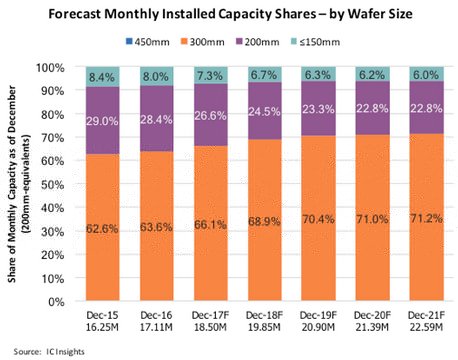
As shown in Figure 1, 300mm wafers represented 63.6% of worldwide IC fab capacity at the end of 2016 and are projected to reach 71.2% by the end of 2021, which translates into a compound annual growth rate (CAGR) of 8.1% in terms of silicon area for processing by plant equipment in the five-year period.

Figure 1
The report’s count of 98 production-class 300mm fabs in use worldwide at the end of 2016 excludes numerous R&D front-end lines and a few high-volume 300mm plants that make non-IC semiconductors (such as power transistors). Currently, there are eight 300mm wafer fabs that have opened or are scheduled to open in 2017, which is the highest number in one year since 2014 when seven were added, says the Global Wafer Capacity report. Another nine are scheduled to open in 2018. Virtually all these new fabs will be for DRAM, flash memory, or foundry capacity, according to the report.
Even though 300mm wafers are now the majority wafer size in use, both in terms of total surface area and in actual quantity of wafers, there is still much life remaining in 200mm fabs, the capacity report concludes. IC production capacity on 200mm wafers is expected to increase every year through 2021, growing at a CAGR of 1.1% in terms of total available silicon area. However, the share of the IC industry’s monthly wafer capacity represented by 200mm wafers is forecast to drop from 28.4% in 2016 to 22.8% in 2021.
IC Insights believes there is still much life left in 200mm fabs because not all semiconductor devices are able to take advantage of the cost savings 300mm wafers can provide. Fabs running 200mm wafers will continue to be profitable for many more years for the fabrication of numerous types of ICs, such as specialty memories, display drivers, microcontrollers, and RF and analog products. In addition, 200mm fabs are also used for manufacturing MEMS-based “non-IC” products such as accelerometers, pressure sensors, and actuators, including acoustic-wave RF filtering devices and micro-mirror chips for digital projectors and displays, as well as power discrete semiconductors and some high-brightness LEDs.
Report Details: Global Wafer Capacity 2017-2021
IC Insights’ Global Wafer Capacity 2017-2021—Detailed Analysis and Forecast of the IC Industry’s Wafer Fab Capacity report assesses the IC industry’s capacity by wafer size, minimum process geometry, technology type, geographic region, and by device type through 2021. The report includes detailed profiles of the companies with the greatest fab capacity and gives comprehensive specifications on existing wafer fab facilities. Global Wafer Capacity 2017-2021 is priced at $4,290 for an individual user license. A multi-user worldwide corporate license is available for $6,990.
Related Semiconductor IP
- UCIe D2D Adapter & PHY Integrated IP
- Low Dropout (LDO) Regulator
- 16-Bit xSPI PSRAM PHY
- ASIL B Compliant MIPI CSI-2 CSE2 Security Module
- SHA-256 Secure Hash Algorithm IP Core