Overview
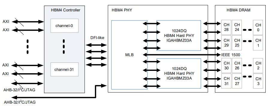
IGAHBMZ03A is a High Bandwidth Memory 4 Physical Layer (HBM4 PHY) that is compliant with JEDEC HBM4 DRAM Specification JESD270-4. Fabricated in the TSMC 3 nm Advanced process node (N3P), it supports the data rate up to 12 Gbps per data pin in the DDR PHY Interface (DFI)-like 1:4 clock frequency ratio (HBM4 controller clock: WDQS = 1:4). The signal and power integrity is analyzed by the GUC design flow to meet all signal and power requirements.
GUC HBM4 PHY includes a hard PHY and a Register Transfer Level (RTL) soft module. The hard PHY, IGAHBMZ03A, includes Command Address (CA) modules, data modules, IO pads, a Phase-Locked Loop (PLL), and Delay-Locked Loops (DLLs). The RTL soft module, also called Miscellaneous Logic Block (MLB), included to work with the hard PHY for functions, such as the training logic, the register controller interface, the Built-In Self-Test (BIST) logic, and the IEEE 1500 function logic.
Learn more about Single-Protocol PHY IP core
UniversalFlash Storage (UFS) was created for mobile applications and computer systems requiring high performance and low power consumption. These systems typically use embedded Flash based on the JEDEC standard eMMC. UFS was defined by JEDEC as the evolutionary replacement for eMMC offering significantly higher memory bandwidth. The standard builds on existing standards such as the SCSI command set, the MIPI Alliance M-PHY and UniPro as well as eMMC form factors to simplify adoption and development.
In this paper, we introduce a new high-level, dataflow programming language called C~ (“C flow”) that further increases productivity by raising the level of abstraction from behavioral descriptions, while overcoming the limitations of C for hardware design. We present the syntax and semantics of this language, and the framework that provides hardware and software code generation. This paper illustrates the benefits of using C~ for hardware design of a IEEE 802.3 MAC, synthesized for FPGA and for 90nm CMOS technology.
Universal Flash Storage (UFS) was created for mobile applications and computer systems requiring high performance and low power consumption. These systems typically use embedded Flash based on the JEDEC standard eMMC. UFS was defined by JEDEC as the evolutionary replacement for eMMC offering significantly higher memory bandwidth. The standard builds on existing standards such as the SCSI command set, the MIPI Alliance M-PHY and UniProSM as well as eMMC form factors to simplify adoption and development.
Since MIPI and MDDI standards both target interfaces to cameras and displays on mobile devices, are two separate standards really needed?
Enter the Inner Sanctum of RapidIO: Part 1
Networking software key to PICMG 2.16 optimization