PCIe with DMA IP
Filter
Compare
62
IP
from
23
vendors
(1
-
10)
-
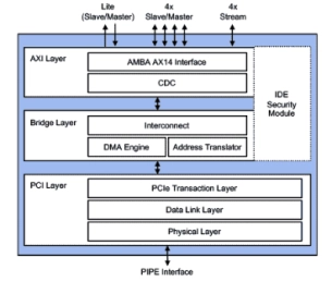
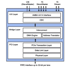
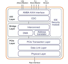
AXI Bridge with DMA for PCIe IP Core
- The AXI Bridge with DMA IP core is the ultimate PCIe DMA IP solution with a powerful mix of multiple industry standard AXI Interfaces.
- AXI Stream interfaces allow continuous data streaming from FPGA to Host or from Host to FPGA. S-AXI Memory mapped interfaces allow easy data access of remote memories in order to realize shared memory access or per to peer applications.
-
PCIe 1.1 Controller supporting Root Port, Endpoint, Dual-mode Configurations, with Built-in DMA and Configurable AMBA AXI Interconnect
- PCIe Interface
- Supported silicon:
- AMBA AXI Interface
- Data Engine and Address translation for PCIe-to-AXI and AXI-to-PCIe transfers
-
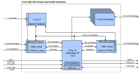
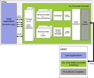
ULL PCIe DMA Controller
- The ULL PCIe DMA Controller is a high-performance, bidirectional data transfer solution. It is designed for seamless communication between FPGAs and host CPUs over PCIe.
- With a round-trip time as low as 585ns*, this IP core empowers developers to maximize resource utilization and achieve ultra-low latency without compromising performance.
-
PCIe DMA Controller (Low Latency)
- Implements standard Transaction layer functions e.g. TLP generation/reception, TLP completion handling and interrupt generation
- Implements 32-bit, 64-bit, 128-bit and 256-bit User application. (Width selection is based on PCIe endpoint interface width)
- PCIe Gen1, Gen2 and Gen3 support.
- Up to 8 independent DMA channels with each channel capable of operating in Block-DMA or Scatter-Gather DMA modes
-
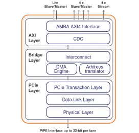
PCIe 2.1 Controller with AXI
- PCIe Interface
- Supported silicon:
- AMBA AXI Interface
- Data Engine and Address translation for PCIe-to-AXI and AXI-to-PCIe transfers
-
PCIe 5.0 Controller with AXI
- Comprises complete PCIe 5.0 interface subsystem with Rambus PCIe 5.0 PHY
- Supports the PCI Express 5.0 rev. 1.0 (32 GT/s), 4.0 (16 GT/s), 3.1/3.0 (8 GT/s) and PIPE (8, 16, 32 and 64-bit) specifications
- Supports the PCI-SIG Single-Root I/O Virtualization (SR-IOV) Specification
- Supports Endpoint, Root-Port, Dual-mode configurations
-
PCIe 4.0 Controller with AXI
- Internal data path size automatically scales up or down (64-, 256- bits) based on link max. speed and width for reduced gate count and optimal throughput
- Configurable pipelining enables full speed operation on Intel and Xilinx FPGA, full support for production FPGA designs up to Gen4 x8/Gen3 x16 with same RTL code
- Stringent implementation of PCIe to AXI Ordering Rules and AXI to PCIe Ordering Rules guarantees AXI deadlock prevention
- Carefully engineered AXI bridge & AXI interconnect allows full performance on AXI interfaces
-
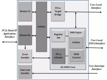
DMA Core for PCIe Hard IP
- TLP Encoding and Decoding
- Completion packet handling done by target bridge
- Integrated Arbiter with round robin fashion
- 32/64 bit AXI stream user interface from PCIe Hard IP depends on no. of PCIe lanes
-
PCIe 3.1 Controller with AXI
- Compliant with the PCI Express 3.1/3.0, and PIPE (16- and 32-bit) specifications
- Compliant with PCI-SIG Single-Root I/O Virtualization (SR-IOV) Specification
- Supports Endpoint, Root-Port, Dual-mode configurations
- Supports x16, x8, x4, x2, x1 at 8 GT/s, 5 GT/s, 2.5 GT/s speeds
- Supports AER, ECRC, ECC, MSI, MSI-X, Multi-function, P2P, crosslink, and other optional features
- Supports many ECNs including LTR, L1 PM substates, etc.

-
PCIe Controller for USB4 with AXI
- Internal data path size automatically scales up or down (64-, 256-, 512- bits) based on link max. speed and width for reduced gate count and optimal throughput
- Configurable pipelining enables full speed operation on Intel and Xilinx FPGA, full support for production FPGA designs up to Gen4 x8/Gen3 x16 with same RTL code – Gen5 support pending
- Stringent implementation of PCIe to AXI Ordering Rules and AXI to PCIe Ordering Rules guarantees AXI deadlock prevention
- Carefully engineered AXI bridge & AXI interconnect allows full performance on AXI interfaces