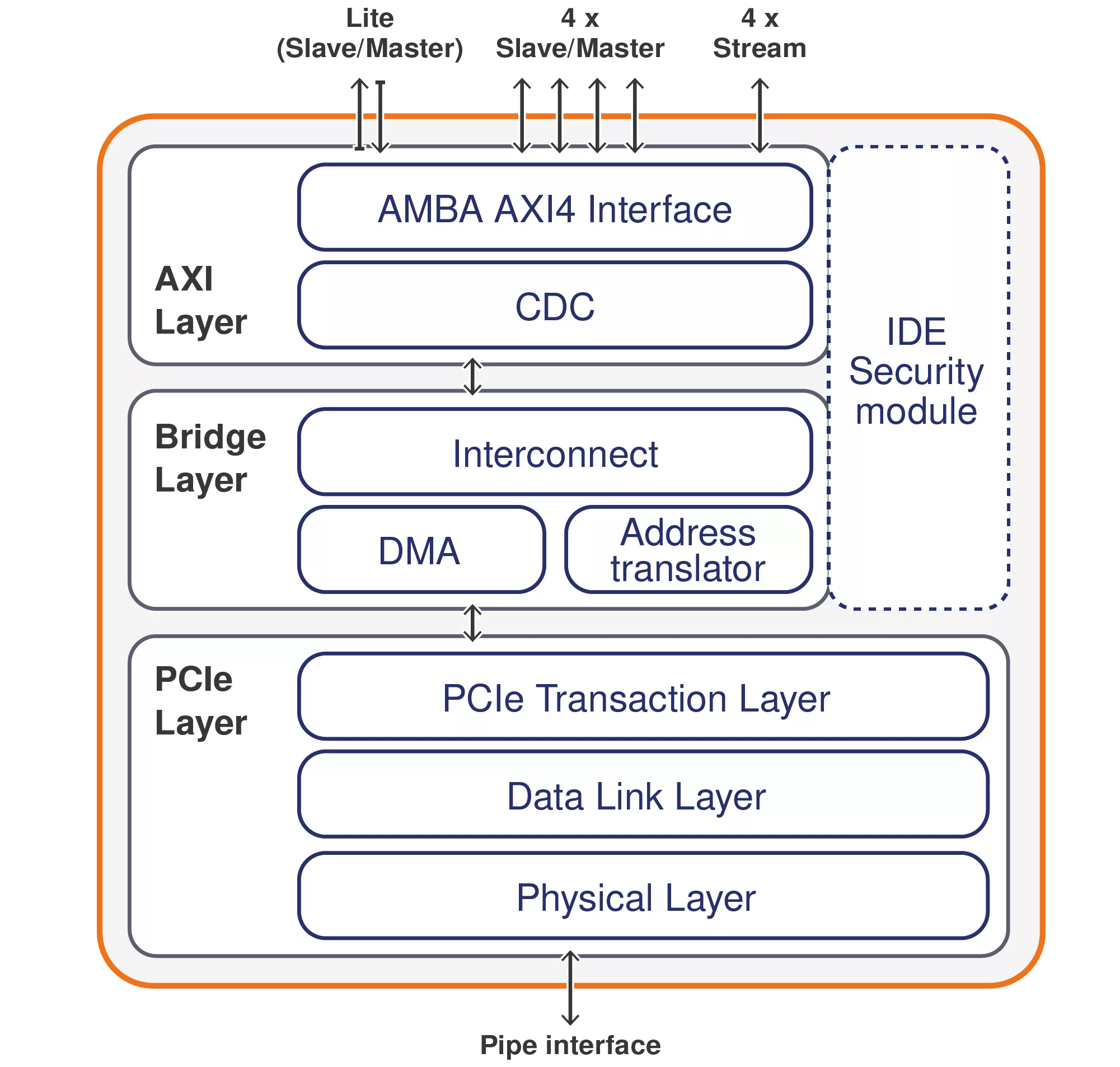
The PCIe 5.0 Controller is designed to achieve maximum PCI Express® (PCIe®) 5.0 performance with great design flexibility and ease of integration. It is fully backward compatible with PCIe 4.0 and 3.1/3.0. A PCIe 5.0 Controller with AXI is also available. The controller delivers high-bandwidth and low-latency connectivity for next-generation applications in artificial intelligence/machine learning (AI/ML), data center, edge, 5G infrastructure and graphics.
How the PCIe 5.0 Controller Works
The PCIe 5.0 Controller is configurable and scalable IP designed for ASIC and FPGA implementation. It supports the PCIe 5.0, 4.0 and 3.1/3.0 specifications, as well as the version 5.x of the PHY Interface for PCI Express (PIPE) specification. The IP can be configured to support endpoint, root port, switch port, and dual-mode topologies, allowing for a variety of use models.
The vendor integrates and validates the PCIe 5.0 Controller with the customer’s choice of 3rd-party PCIe 5.0 PHY.