Peripheral IP for TSMC
Welcome to the ultimate
Peripheral IP
for
TSMC
hub! Explore our vast directory of
Peripheral IP
for
TSMC
All offers in
Peripheral IP
for
TSMC
Filter
Compare
19
Peripheral IP
for
TSMC
from
8
vendors
(1
-
10)
-
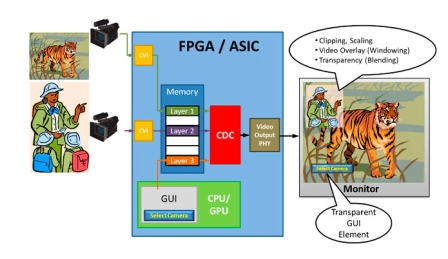
Customizable Display Controller IP
- CDC is a fully Customizable Display Controller IP supporting up to 16k resolutions (4096x4096 pixel) on a MIPI-DPI compliant parallel video output.
- Several features can be configured at synthesis time and programmed at run time.
- The display controller can be applied to e.g. FPGA systems with a resource optimized, application specific feature configuration or to ASIC projects applying a more generic feature set and thus more flexibility.
-
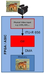
Customizable Video Input controller
- CVI is a fully Customizable Video Input controller IP core.
- The video input controller can be applied to e.g. FPGA systems with a resource optimized, application specific feature configuration or to ASIC projects applying a more generic feature set and thus more flexibility.
-
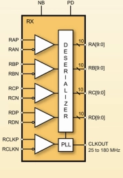
LVDS Deserializer IP
- The MXL-DS-LVDS is a high performance 4-channel LVDS Deserializer implemented using digital CMOS technology.
- Both the serial and parallel data are organized into four channels. The parallel data can be 7 or 10 bits wide per channel. The input clock is 25MHz to 165MHz. The De-serializer is highly integrated and requires no external components.
-
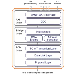
PCIe 3.1 Controller with AXI
- Compliant with the PCI Express 3.1/3.0, and PIPE (16- and 32-bit) specifications
- Compliant with PCI-SIG Single-Root I/O Virtualization (SR-IOV) Specification
- Supports Endpoint, Root-Port, Dual-mode configurations
- Supports x16, x8, x4, x2, x1 at 8 GT/s, 5 GT/s, 2.5 GT/s speeds
- Supports AER, ECRC, ECC, MSI, MSI-X, Multi-function, P2P, crosslink, and other optional features
- Supports many ECNs including LTR, L1 PM substates, etc.
-
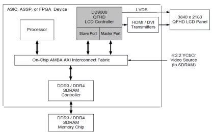
Display Controller – 4K Digital Cinema LCD Panels (AXI4/AXI Bus)
- The DB9000AXI-DCI LCD Controller IP Core interfaces a video image in frame buffer memory via the AMBA 3.0 / 4.0 AXI Protocol Interconnect to a 4K and 2K Digital Cinema Initiative (DCI) High Definition TFT LCD panel
- The video image in frame buffer memory can be 8/10/12-bit YCrCb or RGB, with a Color Space Convert to match the source video to the TFT LCD panel requirements
-
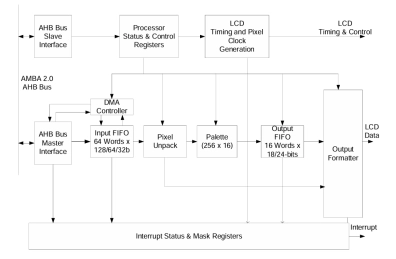
Display Controller - LCD / OLED Panels (AHB Bus)
- The DB9000AHB TFT LCD Controller IP Core interfaces a microprocessor and frame buffer memory via the AMBA 2.0 AHB Bus to a TFT LCD panel.
- In an FPGA, ASIC, or ASSP device, the microprocessor is an ARM processor and frame buffer memory is either on-chip SRAM memory or larger off-chip SRAM or SDRAM.
-
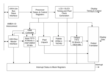
Display Controller - LCD / OLED Panels (AXI4 Bus)
- Advanced display processing, such as Multi-layer Overlay Windows with composition features such as Alpha Blending, Color Space Conversion, 4:2:0 and 4:2:2 YCrCb color with Re sampling & conversion to RGB, Frame Buffer Compression and Hardware Cursor
-
0.035... 100 MHz intermediate-frequency amplifier
- TSMC 65 nm CRN65LP technology
- Differential inputs, outputs
- High frequency 0.035 – 100 MHz
- High linearity
-
Camera Combo Receiver - 2.4Gbps 8-Lane - TSMC 28nm HPC
- The CL12832M8R2JM3KIP2400 is designed to support data rate in excess of maximum 2.4Gbps utilizing SLVS-EC / sub-LVDS / CMOS 1.8V interface specification.
- The CL12832M8R2JM3KIP2400 can change Interface type to same PAD for changing mode.
-
MIPI D-PHY Transmitter 4-Lane (4-Data/1-Clock) 250Mbps
- The CL12631I4T1AS1BIP2500 is an ideal means to link Camera Modules or CMOS Image Sensor (CIS) to Host System.
- The CL12631I4T1AS1BIP2500 converts the input parallel data to the serial data and output it.
- The CL12631I4T1AS1BIP2500 is designed to support maximum 2.5Gbps data rate utilizing mipi-DPHY_specification_v1-2.